3.3. Memory mapped interfaces#
Memory mapped I/O (MMIO) is a method of performing input/output between the central processing unit (CPU) and peripheral devices in a computer. Memory mapped I/O uses the same regular address space to address both memory and I/O devices. The memory and registers of the I/O devices are mapped to (associated with) address values. This means that when an address is accessed by the CPU, it may refer to a portion of the physical RAM, or it may refer to a memory region connected to I/O devices. Thus, the CPU instructions used to access the memory can also be used to access peripheral devices, and areas of the CPU addressable space must be reserved for I/O rather than memory.
3.3.1. The Avalon interface#
The Nios II architecture supports separate instruction and data busses, classifying it as a Harvard architecture cite. Both the instruction and data buses are implemented as Avalon memory mapped (Avalon-MM) master ports that adhere to the Avalon-MM interface specification.
The Nios-II CPU uses the Avalon-MM interface to provide memory mapped read and write access to peripheral devices. The following Avalon interfaces are available:
Avalon Clock Inteface
drives and receives clocks
Avalon Reset Interface
provides reset connectivity
Avalon Memory-Mapped Inteface (Avalon MM)
address-based read/write interface (typical of master-slave connections)
Avalon Streaming Inteface (Avalon ST)
support unidirectional flow of data
Avalon Conduit Interface
for individual signals or group of signals that do not fit into any of the other Avalon Interface types. Conduit signals can be exported to make external connections. That is connections outside of the Nios II system.
Avalon interrupt interface:
allows components to signal events to other components
Fig. 3.1 shows a typical system, highlighting the Avalon-MM slave interface connection to the interconnect fabric.
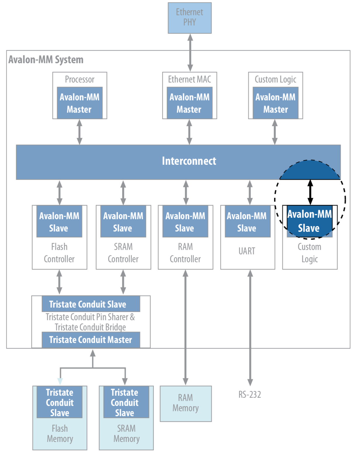
Fig. 3.1 Example of Avalon MM-system#
Avalon-MM interfaces range from simple to complex and typically include only the signals required for the specific component logic that is being implemented. All components must include the Avalon Clock and Reset interfaces. Avalon interfaces are an open standard, that is no license or royality is required to develop and sell products that use, or are based on Avalon interfaces.
More information about the Avalon memory mapped interfaces can be found in Chapter 3 of the Avalon Interface Specificiation document by Intel
3.3.2. An generic Avalon MM module example#
The CPU of a Microcontroller system has different regions of its memory reserved for different perpipherals like GPIO ADC, UART, I2C, SPI, Timers and others. These peripherals occupy an specified address area of the CPU’s memory and can be accessed by using the systems standard read and write operations. The peripherals therefore need to have a set of registers that is part of the addressable memory space of the CPU.
To create a register in VHDL we need to make use of a clocked process statment. Every signal assignment within a rising_edge condition of a clocked proccess will use a flip-flop in one of the FPGAs logic blocks.
library ieee;
use ieee.std_logic_1164.all;

entity test is
  port(
    clk        : in std_logic;
    write_data : in std_logic_vector(31 downto 0)
  );
end entity;

architecture rtl of test is
    signal data_reg : std_logic_vector(31 downto 0);
begin
    p_reg: process(clk)
    begin
        if rising_edge(clk) then
            data_reg <= write_data;
        end if;
    end process;
end architecture;
If the signal assignment is a vector, as in the example above, each bit position of the vector will result in a flipflop. A 32-bit vector will therefore use 32 flip-flops.
The registers can be made addressable by enclosing them in a conditional statement like e.g., the case-statement. To adhere to the Avalon standard we also need to include a write enable.
library ieee;
use ieee.std_logic_1164.all;

entity test is
  port(
    clk          : in std_logic;
    write_enable : in std_logic;
    write_data   : in std_logic_vector(31 downto 0);
    address      : in std_logic_vector(1 downto 0)
  );
end entity;

architecture rtl of test is
    signal data_reg1 : std_logic_vector(31 downto 0);
    signal data_reg2 : std_logic_vector(31 downto 0);
    signal data_reg3 : std_logic_vector(31 downto 0);
    signal data_reg4 : std_logic_vector(31 downto 0);

begin
  p_reg: process(clk)
    begin
      if rising_edge(clk) then
        if write_enable = '1' then
          case address is
            when "00" =>
              data_reg1 <= write_data;
            when "01" =>
              data_reg2 <= write_data;
            when "10" =>
              data_reg3 <= write_data;
            when "11" =>
              data_reg4 <= write_data;
          end case;
        end if;
      end if;
  end process;
end architecture;
The example above implements four writable 32-bit registers. The example can be expanded to also make the registers readable.
library ieee;
use ieee.std_logic_1164.all;

entity test is
  port(
    clk          : in std_logic;
    write_data   : in std_logic_vector(31 downto 0);
    read_data    : out std_logic_vector(31 downto 0);
    address      : in std_logic_vector(1 downto 0);
    read_enable  : in std_logic;
    write_enable : in std_logic
  );
end entity;

architecture rtl of test is
    signal data_reg1 : std_logic_vector(31 downto 0);
    signal data_reg2 : std_logic_vector(31 downto 0);
    signal data_reg3 : std_logic_vector(31 downto 0);
    signal data_reg4 : std_logic_vector(31 downto 0);


begin
  p_reg: process(clk)
    begin
      if rising_edge(clk) then
        -- Write to registers
        if write_enable = '1' then
          case address is
            when "00" =>
              data_reg1 <= write_data;
            when "01" =>
              data_reg2 <= write_data;
            when "10" =>
              data_reg3 <= write_data;
            when "11" =>
              data_reg4 <= write_data;
          end case;
        end if;
        -- Read from registers
        if read_enable = '1' then
          case address is
            when "00" =>
              read_data <= data_reg1;
            when "01" =>
              read_data <= data_reg2;
            when "10" =>
              read_data <= data_reg3;
            when "11" =>
              read_data <= data_reg4;
          end case;
        end if;
      end if;
  end process;
end architecture;
The last modification that is needed to adhere to the Avalon standard is to add a reset. For this example an asynchronous active low reset will be used. Since this is an asynchronous reset, it must also be added to the sensitivity list of the process.
library ieee;
use ieee.std_logic_1164.all;

entity test is
  port(
    clk          : in std_logic;
    arst_n       : in std_logic;
    write_data   : in std_logic_vector(31 downto 0);
    read_data    : out std_logic_vector(31 downto 0);
    address      : in std_logic_vector(1 downto 0);
    read_enable  : in std_logic;
    write_enable : in std_logic
  );
end entity;

architecture rtl of test is
    signal data_reg1 : std_logic_vector(31 downto 0);
    signal data_reg2 : std_logic_vector(31 downto 0);
    signal data_reg3 : std_logic_vector(31 downto 0);
    signal data_reg4 : std_logic_vector(31 downto 0);


begin
  p_reg: process(areset_n, clk)
    begin
      if areset_n = '0' then
        data_reg1 <= (others => '0');
        data_reg2 <= (others => '0');
        data_reg3 <= (others => '0');
        data_reg4 <= (others => '0');
      elsif rising_edge(clk) then
        -- Write to registers
        if write_enable = '1' then
          case address is
            when "00" =>
              data_reg1 <= write_data;
            when "01" =>
              data_reg2 <= write_data;
            when "10" =>
              data_reg3 <= write_data;
            when "11" =>
              data_reg4 <= write_data;
          end case;
        end if;
        -- Read from registers
        if read_enable = '1' then
          case address is
            when "00" =>
              read_data <= data_reg1;
            when "01" =>
              read_data <= data_reg2;
            when "10" =>
              read_data <= data_reg3;
            when "11" =>
              read_data <= data_reg4;
          end case;
        end if;
      end if;
  end process;
end architecture;
These registers are now available for access from the CPU and can be use to control and communicate with logic inside the module. A more specific example is shown in the next example, where the memory mapped register is used to control a basic timer.
3.3.3. A basic timer module example#
The example below demonstrates how this could be done for a basic timer. One register is used as a command register while another is used as the timer. The command register has to active bit positions: reset_timer (bit pos. 1) and run (bit pos 0). These bits are used to control the start, stop, and reset of a counter. When writing a ‘1’ in bit position 0 (run bit), the register data_reg_timer will increment on every clock cycle. This counter can be stopped by writing a ‘0’ to the same bit position, or by writing a ‘1’ to bit position 1 (reset_timer).
As long a the reset bit is enabled, the counter will remain in a reset condition. The counter can be brought out of reset with two differen methods. Can you think how this can be done?
Answer
Either, the counter can be brought out of the reset condition from software. That is, the software writes a ‘0’ to the corresponding bit position. Or, this can be done automatically from the control logic of the module. The solution in this example uses the latter method. By simply adding a statement at the top process within the rising_edge condition that always writes ‘0’ to the reset bit position. This works because the process evaluates the statements sequentially, and it is always the last assignment to a signal within a process that is valid. Thus, in this case, the alias signal reset_timer is first scheduled to be assigned ‘0’. Then if the if a ‘1’ is assigned to the same bit position within the write_enable = '1' condition, this will be the last assignment that will be updated and valid for the present clock cycle. On the following clock cycle, the write_enable = '1' condition is no longer valid, and thus the default assignment reset_timer <= '0' is the only valid assignment.
A basic timer can be used to measure the number of clock cycles for a certain operation in software. The counter is first started. Then the respective task is performed before the timer is stopped. By reading the value in the data_reg_timer and multiplying this by the known clock period, the duration of the performed tasks can be measured.
library ieee;
use ieee.std_logic_1164.all;
use ieee.numeric_std.all;

entity timer_module is
  port(
    clk          : in std_logic;
    arst_n       : in std_logic;
    write_data   : in std_logic_vector(31 downto 0);
    read_data    : out std_logic_vector(31 downto 0);
    address      : in std_logic_vector(1 downto 0);
    read_enable  : in std_logic;
    write_enable : in std_logic
  );
end entity;

architecture rtl of timer_module is
  -- Command register
  -- Bit 0: Run bit ('1': timer acitve, '0': timer inactive)
  -- Bit 1: Reset bit ('1': reset timer)
  -- Bit 2-31: Unused
  signal data_reg_cmd : std_logic_vector(31 downto 0);
  -- Timer register. This operates as a 32 bit counter.
  signal data_reg_timer : unsigned(31 downto 0);
  -- Aliases for more readable access to individual bits in registers
  alias run : std_logic is data_reg_cmd(0);
  alias reset_timer : std_logic is data_reg_cmd(1);

begin
  -- Processor interface memory mapped process
  -- Only the data_reg_cmd is writable from the cpu
  -- The data_reg_timer is controlled from the p_timer process
  -- but can be read by the processor software
  p_reg: process(areset_n, clk)
    begin
      if areset_n = '0' then
        data_reg_cmd <= (others => '0');
      elsif rising_edge(clk) theni
        -- default value to reset the timer.
        reset_timer <= '0';
        -- Write to registers
        if write_enable = '1' then
          case address is
            when "00" =>
              -- Write data to the command register from sofware
              -- If reset timer bit position is written, this will
              -- take precedence over the default assignment above.
              data_reg_cmd <= write_data;
          end case;
        end if;
        -- Read from registers
        if read_enable = '1' then
          case address is
            when "00" =>
              read_data <= data_reg_cmd;
            when "01" =>
              -- Read the timer/counter value. Convert from unsigned to slv.
              read_data <= std_logic_vector(data_reg_timer);
          end case;
        end if;
      end if;
  end process;

  -- Timer process
  -- When the software writes a '1' to bit position 0
  -- in the data_reg_cmd, the counter increments on
  -- every clock edge. To stop the counter, the software
  -- has to write a '0' to the same bit position.
  -- To reset the timer, the software must toggle the bit
  -- position 1 in the data_reg_cmd. That is, first write a '1',
  -- followed by a '0'.
  p_timer: process(clk)
    begin
      if rising_edge(clk) then
        -- Reset timer has priority over run. This means
        -- that the timer can be reset without first stopping
        -- the timer.
        if reset_timer = '1' then
          data_reg_timer <= (others => '0');
        elsif run = '1' then
          data_reg_timer <= data_reg_timer + 1;
        end if;
  end process;


end architecture;
Comment to video
From 8:22 this video covers the implementation of an I2C-master, which was used previously in this course. Although we are using a UART controller for the embedded systems project in 2021, the explanations and general concepts are still highly relevant.