2.11. Metastability and synchronization#
Metastability is a phenomenon that can lead to system failure in digital devices such as FPGAs. It can occur when signals are transferred between registers of unrelated or asynchronous clock domains, as shown in Fig. 2.34. Or when the combinational path between to registers is too long for the signal to become stable at the input of the next register in time for the next transition on the clock, see Fig. 2.35.
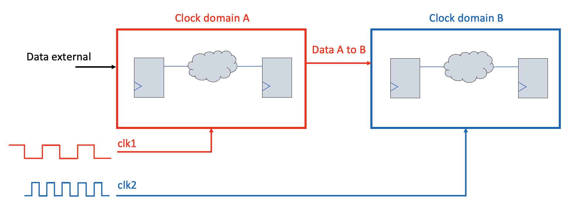
Fig. 2.34 If clk1 and clk2 are skewed/sliding with respect to each other (or of different frequency or unrelated), the data received in clock domain B may violate the setup and hold time of the input register in this domain. The same is the case for an external and asynchronous signal arriving into clock domain A.#
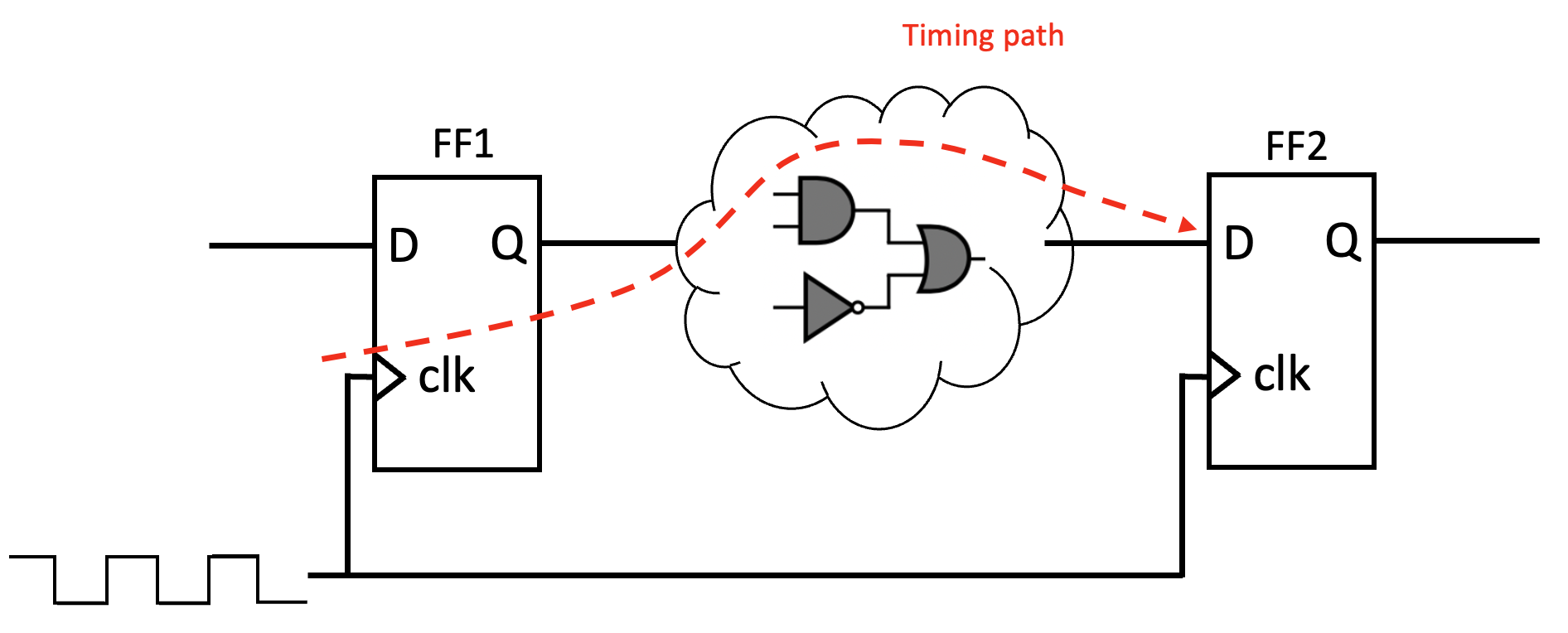
Fig. 2.35 If the combinational path is to long for the signal to arrive at the input of the second register in due time of the next active edge of the clock, this violates the timing requirements of the design, and timing closure can not be met.#
2.11.1. Setup and hold times#
A flip-flop has a requirement to when new data may change with respect to the active edge of the clock. That is, the input of the flip flop must have changed and be stable at a given time before the clock edge, and remain stable for a given time after the clock has changes. This is referred to as setup-time (\(t_s\)) and hold-time (\(t_h\)) respectively. If this requirement is not met it is referred to as a “timing violation”. It may lead to a metastable state of the flip-flop where its output is unstable and unpredictable for a short amount of time, before it eventually and randomly settles to either its previous value or to its new value.
setup-time (\(t_s\)): is the minimum amount of time before the clock’s active edge that the data must be stable for it to be latched correctly.
hold-time (\(t_h\)): is the minimum amount of time after a clock’s active edge during which the data must be stable.
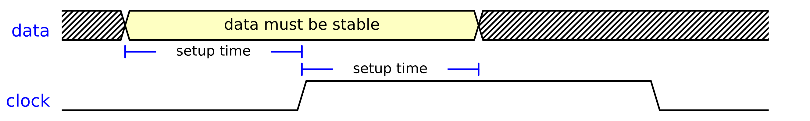
Fig. 2.36 Wave diagram illustrating setup time and hold time with respect to the data and clock signals.#
When a signal is transferred between registers, the input of the receiving register must be stable at least \(t_s\) before the capturing edge of the clock. This is demonstrated in the wave diagram in Fig. 2.37.
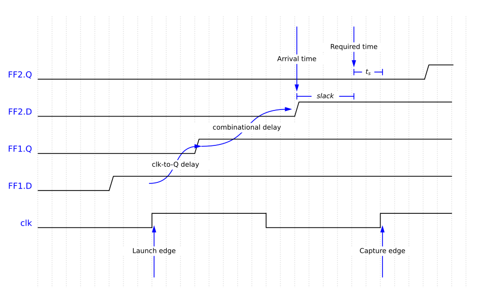
Fig. 2.37 Data from FF1 much reach the input of FF2 well before the setup requirement. The labels correspond to the labels used in Fig. 2.35#
The value at the input of the first register (FF1.D) is captured at the launching edge of the clock. This value then starts the race of reaching the input of the next register in time to be captured at the next active clock edge. The clk-to-Q delay corresponds to the time it takes for the input value to propagate through the register from D to Q. The signal then has to propagate through the combinational path between the two registers before it arrives at the input FF2.D. If the arrival time is before the required setup time \(t_s\), the signal value is correctly captured by the second register. We say that the timing requirement for that path is met with a corresponding positive slack. If the arrival time is after the required time, the timing requirement is not met, and we have a negative slack. In this case, a redesign of the path may be necessary.
2.11.2. Pipelining#
For example, the timing can be improved by splitting the combinational path in two shorter paths separated by an additional register. This will delay the signal by one clock cycle, but with the two shorter combinational paths, the signal is now correctly propagated through the logic without risking a metastable state. This solution is also known as a pipelining and is conceptually illustrated in Fig. 2.38.
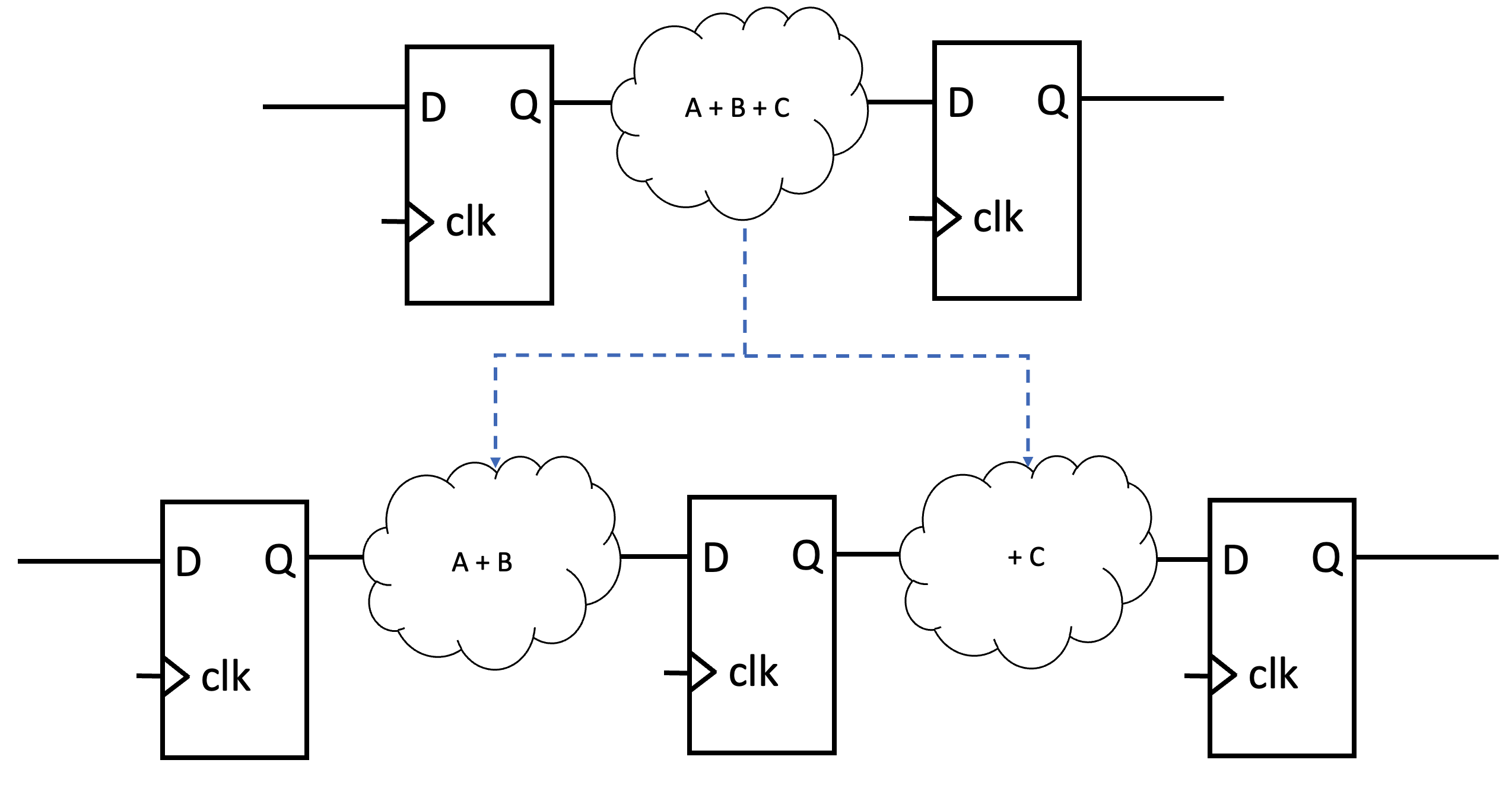
Fig. 2.38 Assume that combinational logic neede to compute A + B + C is too long for the signal to reach the input of the second register in time for the next clock edge. The computation can then be split into to paths separated by a register. Individually, each computation now creates a shorter combinational path capable of meeting the timing requirements.#
2.11.3. Synchronization#
The probability of metastability can be reduced by first aligning the incoming signal to the clock of the local clock domain. By bringing the incoming signal through two registers, as illustrated in Fig. 2.39, the signal is effectively synchronized to the clock of the receiving clock domain.
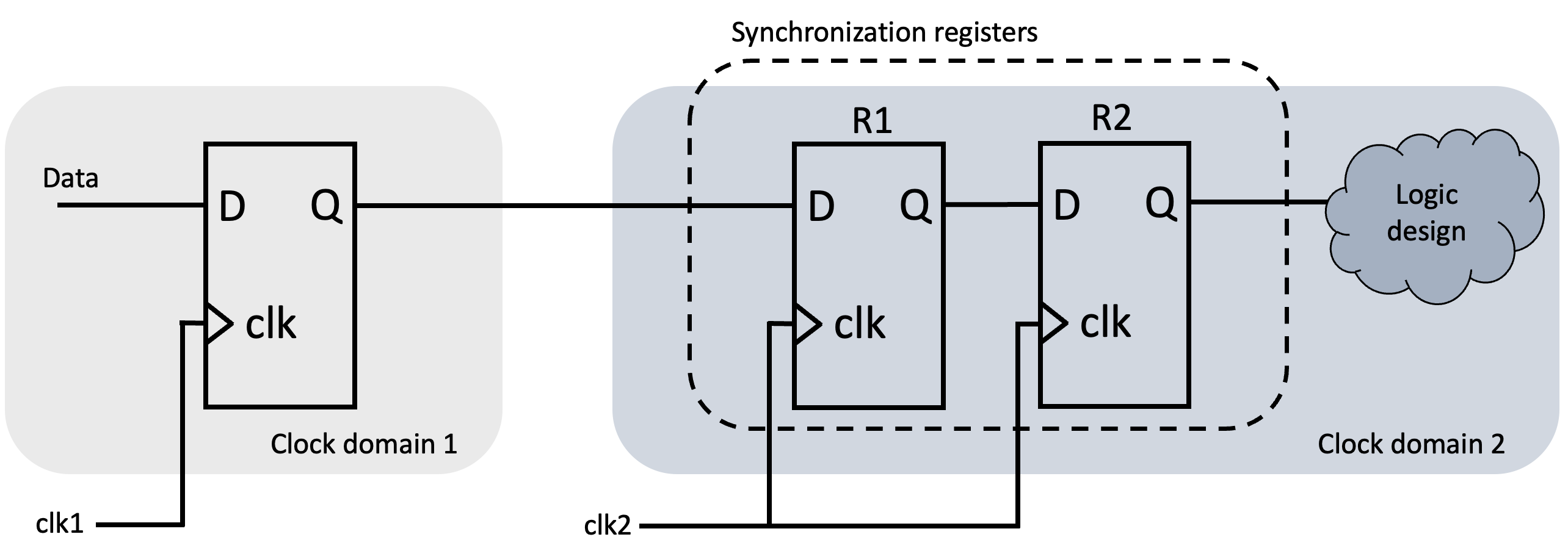
Fig. 2.39 An accepted rule of thumb to reduced the probability of metastability is to use to synchronization registers to align the incoming signal with the local clock.#
The wave diagram in Fig. 2.40 shows how the synchronization registers work.
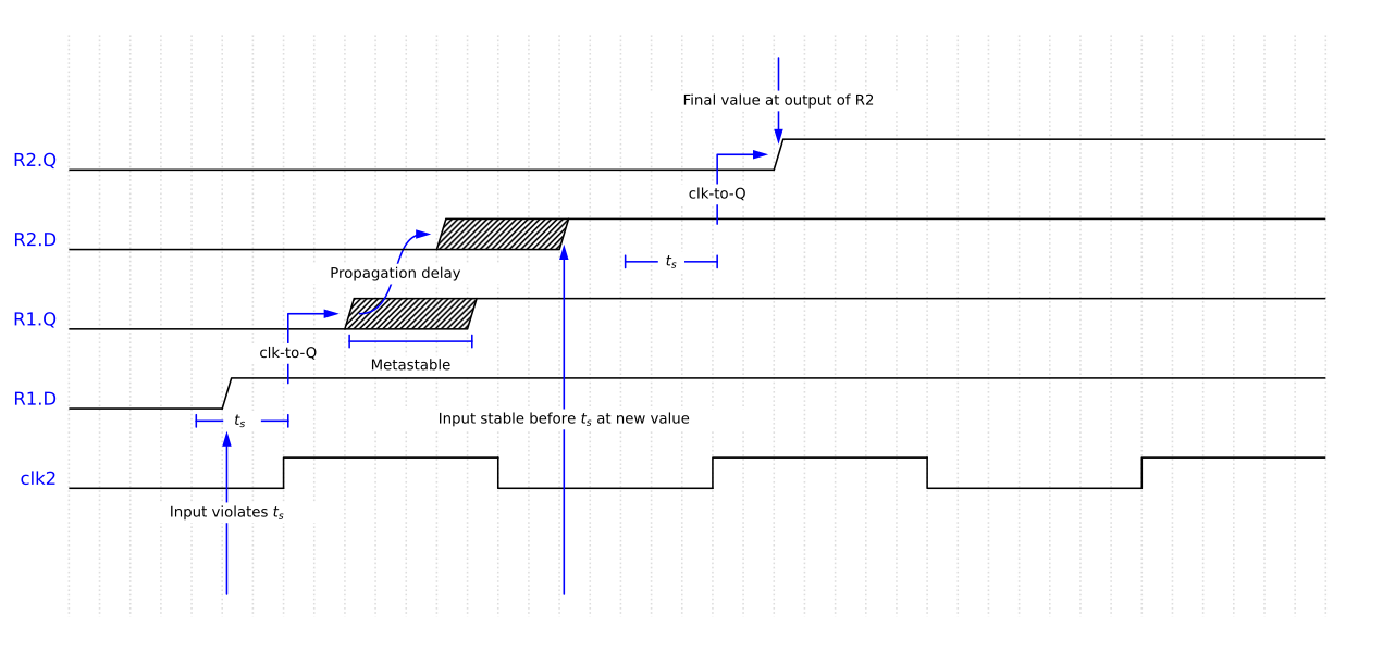
Fig. 2.40 Wave diagram showing the propagation of an incoming signal through the two synchronization registers. In this example the metastable output of the first synchronization register settles at the new value. Fig. 2.41 shows the case when it settles at the old value.#
Here the incoming signal changes too close to the clock edge and therefore violates the setup time of the first register R1. This brings the output of R1 into a metastable state, from which it is impossible to predict the resulting value. In this example the output eventually settles at the new value. A short propagation delay later, this new value then arrives at the input of R2. As long as the metastable state and propagation delay is shorter than the clock cycle and meets the setup time of the second register, R2 can correctly clock through the new value. The solution allows the first of the two registers to become metastable while the second register shields that metastable state from the internal logic. No logic must be introduced in the path between the two synchronization registers.
The example above shows what happens if the metastable state returns to the new value. However, what if the metastable state returns to the old value. This is illustrated in the wave diagram in Fig. 2.41.
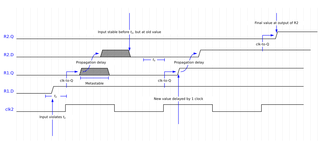
Fig. 2.41 Wave diagram showing the propagation of an incoming signal through the two synchronization registers. In this example the metastable output of the first synchronization register settles at the old value. Fig. 2.40 shows the case when it settles at the new value.#
Using synchronization registers to align the incoming signal with the local clock only works if the clock frequency of the local clock domain is higher than clock domain driving the incoming signal. If the driving clock domain runs at a higher frequency, the receiving clock domain will not be able to capture the incoming value before it changes to a new value. In this case a different synchronization mechanism is required, such as adding handshake signals. This is however, outside the scope of this course.
2.11.4. Edge detection#
Sometimes an external signal like for instance a key press is used to trigger an event in the FPGA design. A key press is an asynchronous signal with a duration much longer than the clock frequency of the FPGA design. In this course we are using a 50 MHz clock, which corresponds to clock period of 20 ns. If you are reactive, you may be able to reduce the duration of a key press to a few hundreds of milliseconds. It is clear that if you press the key and simply trigger on the level of that signal, the internal event will be much longer than a single clock period. If this signal is used to trigger a single increment of a counter, the counter will increment by a lot more than one.
architecture rtl of edge_detection is
begin

  p_reg: process(clk)
    begin
      if rising_edge(clk) then
        -- trigger on the external active low signal signal
        if enable = '0' then
          counter <= counter + 1;
        end if;
      end if;
  end process;

end architecture;
The VHDL description above will result in the behaviour shown in Fig. 2.42
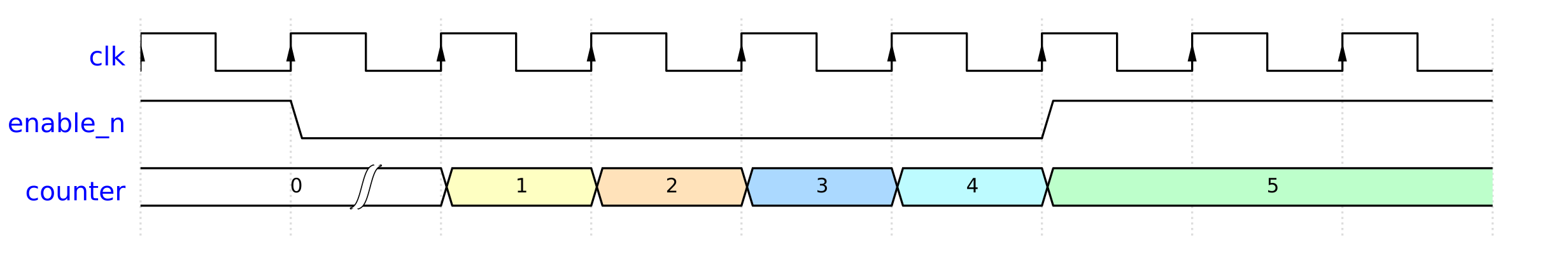
Fig. 2.42 If the enable signal has a longer duration than the counter, the counter will increment by more than one.#
To avoid this we need to trigger the counter on one of the edges of the enable signal. A first natural idea would be to use one of the functions rising_edge() and falling_edge(). However, these functions are only allowed to be used on clock signals. The synthesis tools interpret the argument to these functions as a dedicated clock signal. They can therefore not be used on regular logic signals in the design. Instead, we will have to design custom edge detection logic. By bringing the incoming enable signal through a register it is possible to detect the transition on the signal by monitoring each side of the register. If we want to detect the falling edge of the signal, the required condition is that the incoming signal changes to ‘0’ while the output of the register not yet has been updated with this new value. By inverting the incoming signal and comparing it to the output of the register through an AND-gate, a one clock cycle long pulse is generated. The corresponding circuit and resulting wave diagram is shown in Fig. 2.43 and Fig. 2.44 respectively.
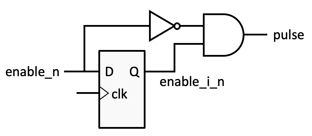
Fig. 2.43 Single shot pulse generator.#
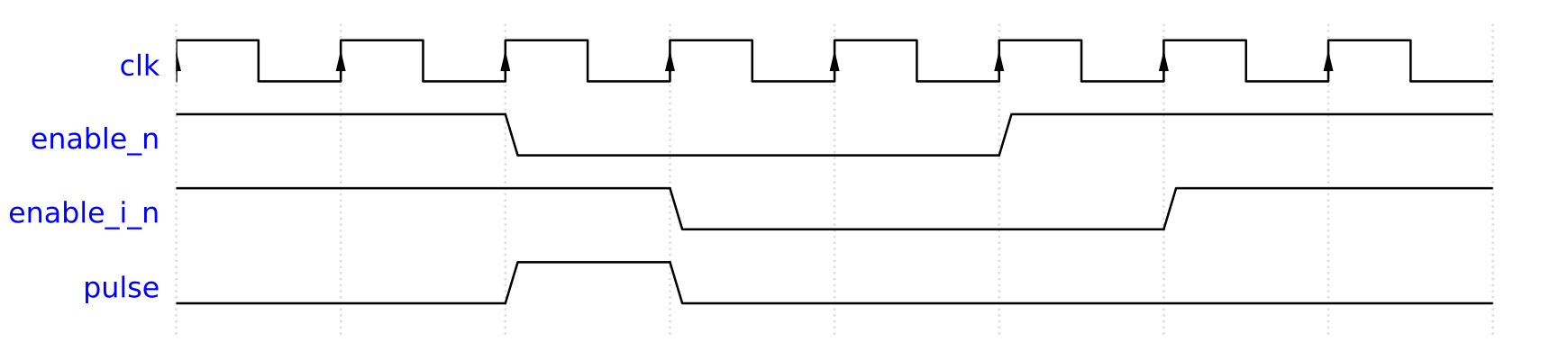
Fig. 2.44 Wave diagram for the single shot pulse generator.#
The corresponding VHDL description is shown below.
architecture rtl of edge_detection is
  signal enable_i_n : std_logic;
begin

  p_reg: process(clk)
    begin
      if rising_edge(clk) then
        enable_i_n <= enable_n;
      end if;
  end process;

  -- Create the falling edge detection and thus
  -- a pulse with a duration of one single clock
  -- cycle
  pulse <= not enable_n and enable_i_n;

  -- If you want to create a pulse on the rising edge
  -- of the input enable signal, place instead the inverter
  -- at the output of the register, effectively inverting
  -- the enable_i_n signal as shown in the commented line
  -- below.
  -- pulse <= enable_n and not enable_i_n;

end architecture;
This circuit assumes that the incoming enable signal already is synchronized to the same clock that is used to drive the register. However, since this signal is an external key press, it must also first be synchronized into the local clock domain, using synchronization registers as shown earlier. The resulting logic can be seen in Fig. 2.45.
This results in pulse on the output with a duration of a single clock cycle, which in turn can be used as an enable signal for a counter or any other logic requiring a single pulse. You will use approach to create an enable signal for the counter design in EX3: 4-bit up-counter.
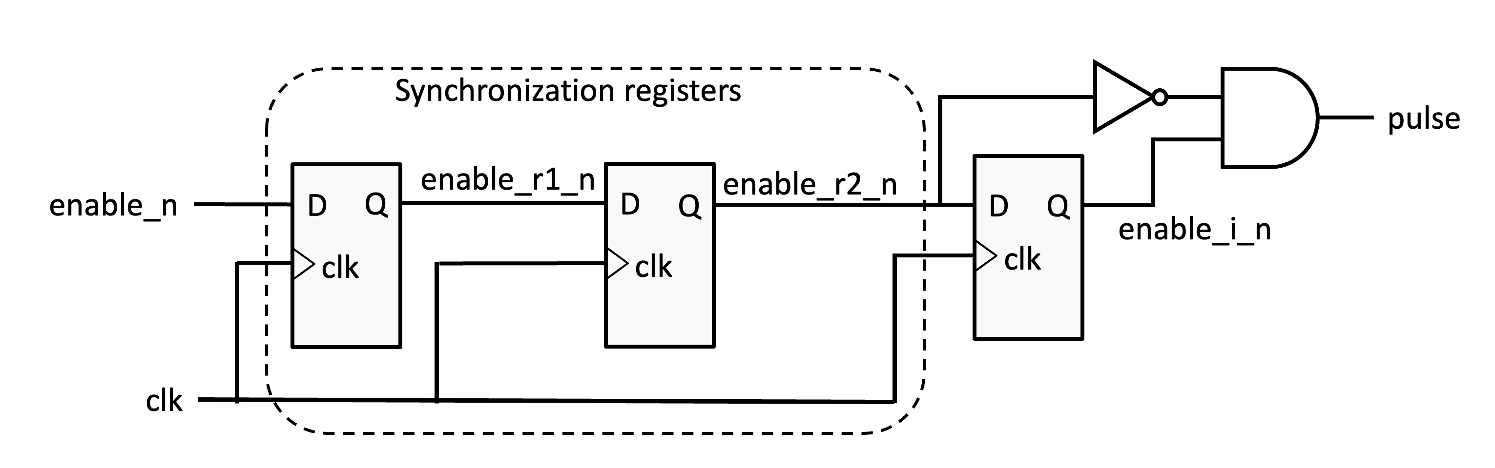
Fig. 2.45 The two input registers synchronizes the incoming signal to the local clock domain.#
The VHDL implementation of the diagram above is shown below:
library ieee;
use ieee.std_logic_1164.all;

-- This module detects the falling edge of the asynchronous
-- active low incoming enable_n signal and generates a single
-- active high output pulse with a duration equal to the length of
-- one clock cycle of the incoming clock clk.
entity edge_detection is
port (
  clk : in std_logic;
  enable_n : in std_logic;
  pulse : out std_logic
);
end edge_detection;


architecture rtl of edge_detection is

  -- Signal for the two synchronization registers
  signal enable_r1_n : std_logic;
  signal enable_r2_n : std_logic;
  -- Signal for the edge detection register
  signal enable_i_n : std_logic;
begin

  -- This process the 3 registeres through
  -- which the input enable signal is clocked to
  -- to first synchronize the signal and then to add
  -- a register used for the combinational edge detection logic
  -- described in the separate statement below.
  p_synchronization: process(clk)
    begin
      if rising_edge(clk) then
        -- First bring the input signal through the
        -- two synchronization registers
        enable_r1_n <= enable_n;
        enable_r2_n <= enable_r1_n;
        -- Additional register for edge detection functionality
        enable_i_n <= enable_r2_n;
      end if;
  end process;

  -- Create the falling edge detection and thus
  -- a pulse with a duration of one single clock
  -- cycle
  pulse <= not enable_r2_n and enable_i_n;

end architecture;
The figure below shows the corresponding wave diagram. The signal enable_n is shown as an asynchronous signal, changing indpendently of the clock.
Fig. 2.46 Wave diagram for the single shot pulse generator.#
What would happen if you wrote the statement for generating the pulse signal inside the process?
Adding the statement to the synchronous process will result in an additional register at the end of the signal path. This will delay the pulse signal by one clock cycle. This may or may not be important, depending on the application. In our case this is not needed. The corresponding code and schematic is shown below.
p_synchronization: process(clk)
    begin
      if rising_edge(clk) then

        enable_r1_n <= enable_n;
        enable_r2_n <= enable_r1_n;
        enable_i_n <= enable_r2_n;

        -- Each statement within a synchronous process will create a register
        pulse <= not enable_r2_n and enable_i_n;

      end if;
  end process;
Fig. 2.47 Four registers will be created by the code above, one for each statement.#
Supplementary suggested reading:
The Altera white paper on understanding metastability in FPGAs.
Chapter 7, section 7.1.1 and 7.1.2 in LaMeres [LaM19].