P2: Microcontroller system#
In this part of the project you will build and implement the soft core processor that will be used to read out data from the digital accelerometer sensor.
Preparation
Before continuing you should work through the example described in EX5: A basic Nios II system, EX6: Accessing Nios II memory mapped modules and EX7: Nios II interrupt handling.
The system described and developed in these examples will be used in this part to build the final system.
The microcontroller system will now be expended with the remaining components needed for the final system. These are:
The UART module from P1: UART controller to communicate between the microcontroller system and the host PC.
An SPI module to communicate with the accelerometer.
An Interval Timer module to provide a periodic tick every 1 ms – to be used when adding the real-time kernel in P3: RTOS.
In addition the ADXL345 accelerometer [Deva] has two interrupt lines that will be connected to the system. A PIO module was already used in EX7: Nios II interrupt handling to handle an interrupt from an external push button. The two interrupt lines can easily be added to this module by increasing the number of inputs from 1 to 3.
An overview of the full system is shown in Fig. 53.
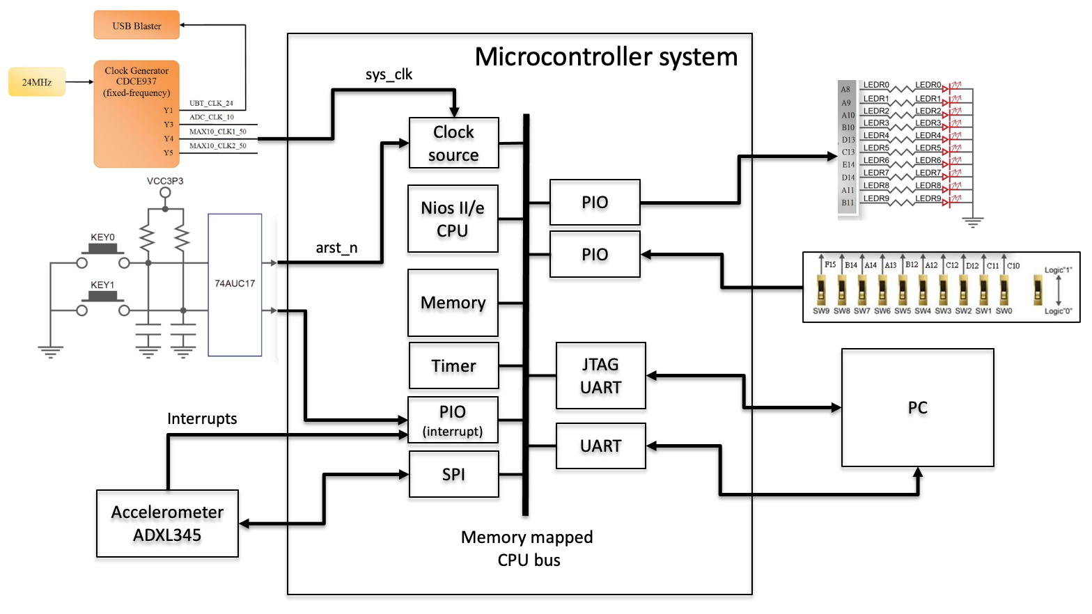
Fig. 53 Overview of full Nios II system for the FYS4220 project.#
The two main tasks in this part of the project is to:
Update the hardware of the microcontroller system in Hardware
Test the UART and SPI interface in Software
You will start by integrating the UART module developed in P1: UART controller.
Useful check list
During the hardware development part it is important that you remember to:
Regenerate the microcontroller system’s HDL description files after updating the system in the Platform Desginer.
Modify the top level VHDL file to include the new Nios II system including new ports for UART, SPI, and interrupt lines.
Update and rerun the pinning Tcl-script to assign the correct FPGA pin numbers to the respective ports.
Recompile the Quartus project.
Before you develop the software application it is important that you remember to regenerate the board support package files to reflect this changes for the software application.
Hardware#
With today’s large FPGA designs it can be difficult to design all the needed functionality from scratch. Using already developed blocks for parts of the design, where these are available, is therefore recommend. These blocks are often referred to as Intellectual Properties (IPs). A large number of IPs are available from the FPGA manufacturers or from third-party supplier. When choosing the various components to add to your Nios II system, like for example the PIO modules, these are in fact IP components provided by Intel. IP components may be free and open source or commercial and available for a fee. In cases where no appropriate IP module is available, or considered to be too expensive, the only solution is to develop your own IP. The following sections will demonstrate how to make the UART controller available as an IP in the Platform Designer’s IP catalog, and how to include and use an already available SPI core from the IP catalog.
Platform designer#
Creating the UART IP#
In order to describe and package IP components for use in the Nios II system, you must create a Hardware Definition File (_hw.tcl) which will describe your component, its interfaces, and associated HDL files. This file will be used by the Platform Designer to identify and include the module in the IP catalog. The Platform designer tool provides a Component Editor GUI to help create a simple _hw.tcl file. A component can have any number of interfaces in any combination. Each interface represents a set of signals that you can connect within the Platform designer, or export outside of the system (e.g., our RX and TX ports). For this project and for uart.vhd component designed in P1: UART controller, the following interfaces will be used:
a memory mapped interface to provide the Nios II CPU access to the components register space
Signals: we, re, wdata, rdata, addr
a clock interface
Signals: clk
a reset interface
Signals: arst_n
a conduit interface to export the RX and TX ports
Signals rx, tx
an interrupt interface
Signals: irq
If you continue to work with the example from sections EX5: A basic Nios II system, EX6: Accessing Nios II memory mapped modules and EX7: Nios II interrupt handling, you should now copy your UART source files into the hdl directory.
In Platform designer start the Component editor: File->New Component. Give the new component a name and provide other relevant information similar to what is shown in Fig. 54.
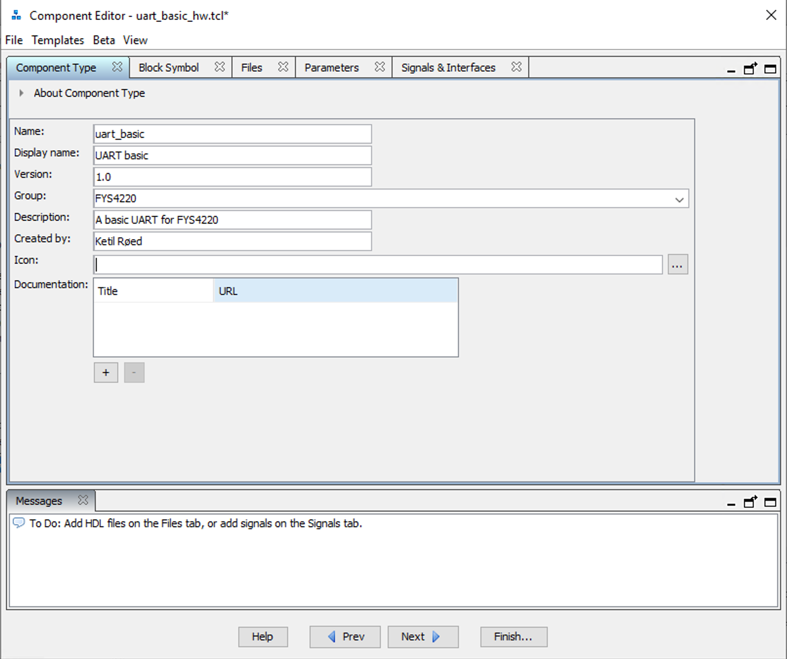
Fig. 54 Component editor. Specify component information.#
Change to the Files tab and and click the Add File… button under the first section Synthesis Files. Navigate to the hdl directory and add your all your UART source files as shown in Fig. 55.
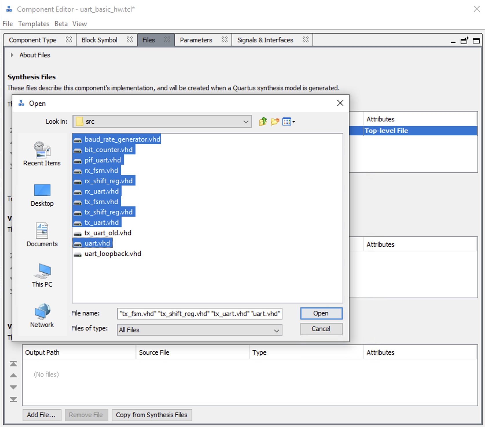
Fig. 55 Add the UART source files.#
Note
Note that you may have different files and filenames than shown in the figure. Make sure to add all of YOUR UART design files.
Make sure to set the correct top level file. For the example here this is uart.vhd as shown in Fig. 56.
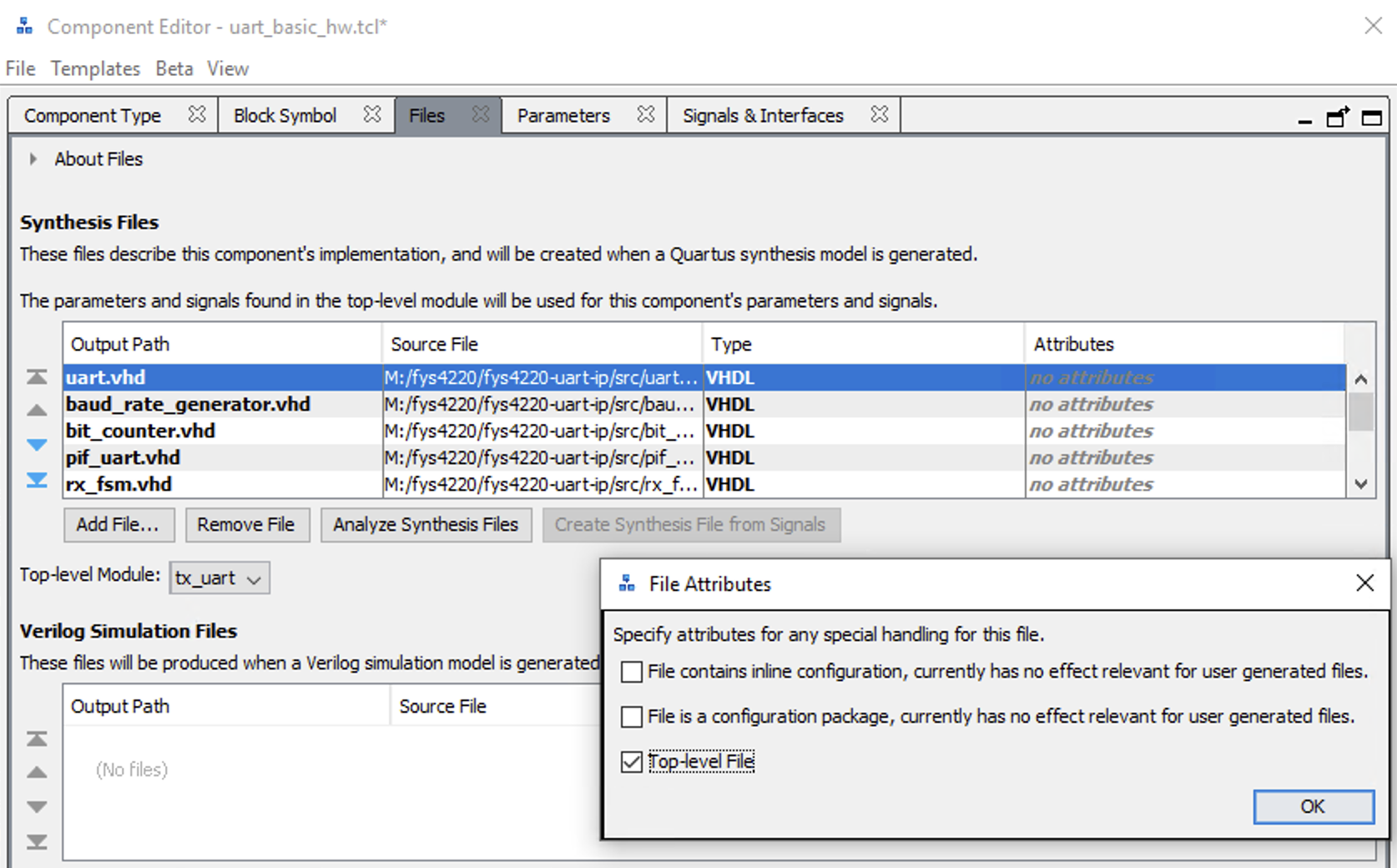
Fig. 56 Click on the no Attributes column for the uart.vhd file and choose Top-Level File.#
Then click the Analyse Synthesis files button to analyse the source files as shown in Fig. 57. This process will identify the top-level file as well as making an attempt to identify and assign the appropriate interfaces.
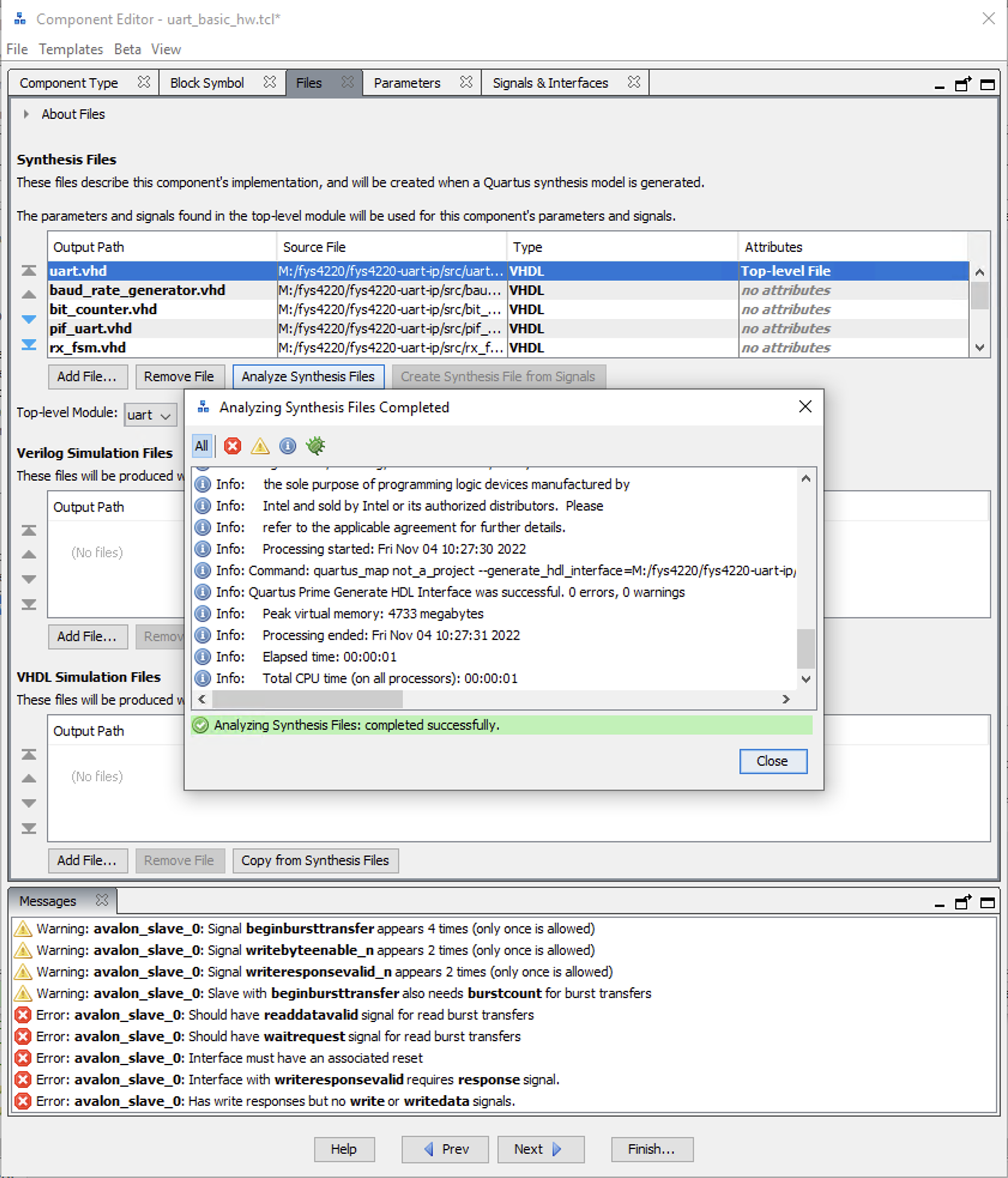
Fig. 57 Analyze the VHDL source files.#
A number of warnings and error messages will appear after the analysis has been completed. If you change to the Signals and interfaces tab, you will see the list of interfaces and assosicate signals that has been identified. Fig. 58 shows that only a few signals and interface has been sucessfully identified. You therefore need to manually add the relevant interfaces and types, and sort the signals under their associated interface.
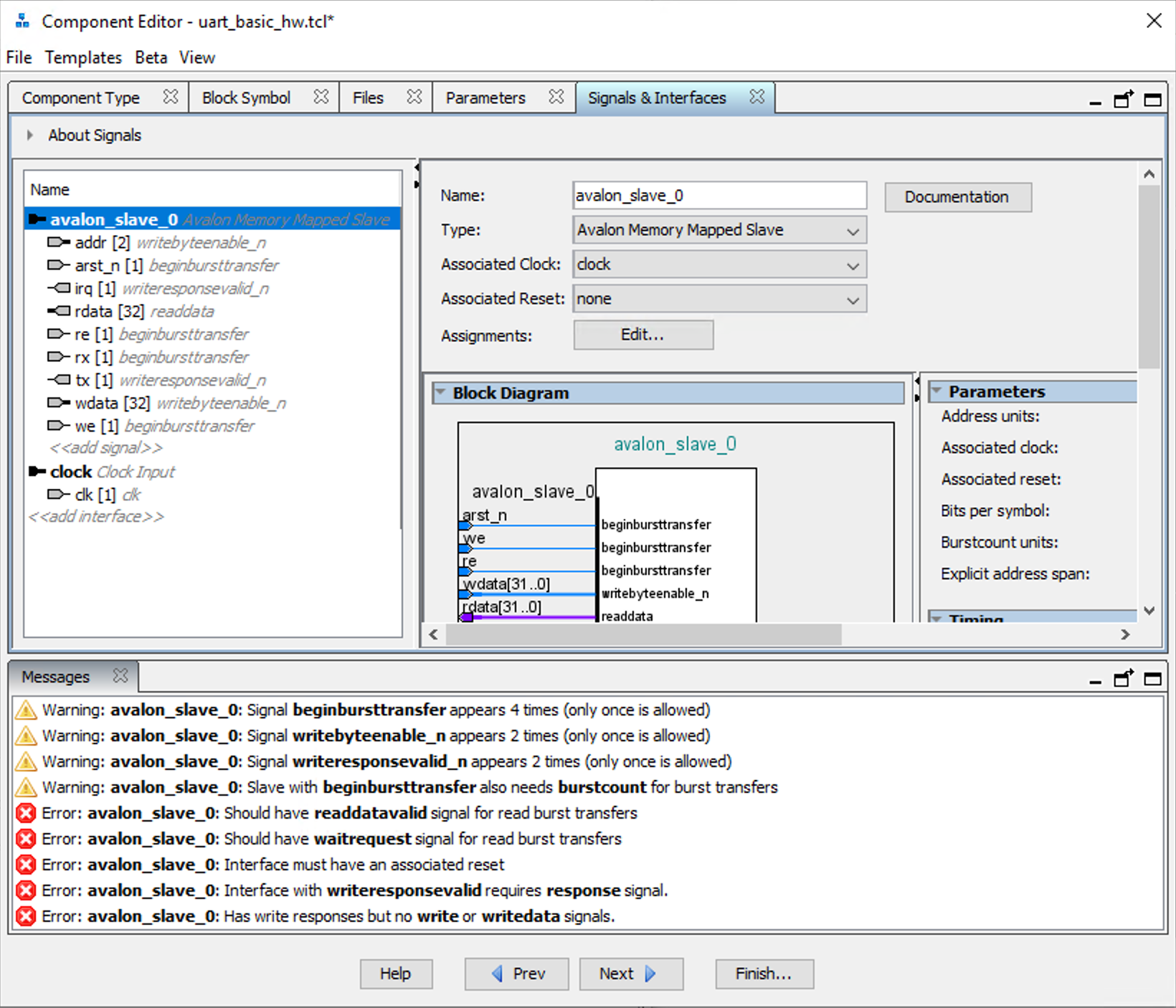
Fig. 58 Project component signals#
First, add the reset input interface. Click the <<add interface>> field at the bottom of the list, and choose Reset Input as shown in Fig. 59.
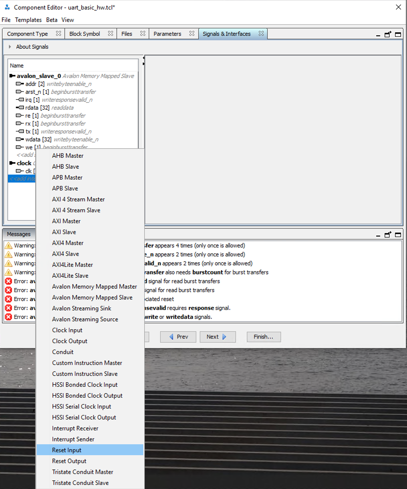
Fig. 59 Add a reset interface.#
The reset interface must be configured with the correct signal type. Since we have an active low reset we choose reset_n as shown in Fig. 60. The arst_n has been incorrectly identified as a beginbursttransfer signal associated with the Avalon slave interface. The arst_n signal must therefore be moved to the reset interface by a click and drag operation.
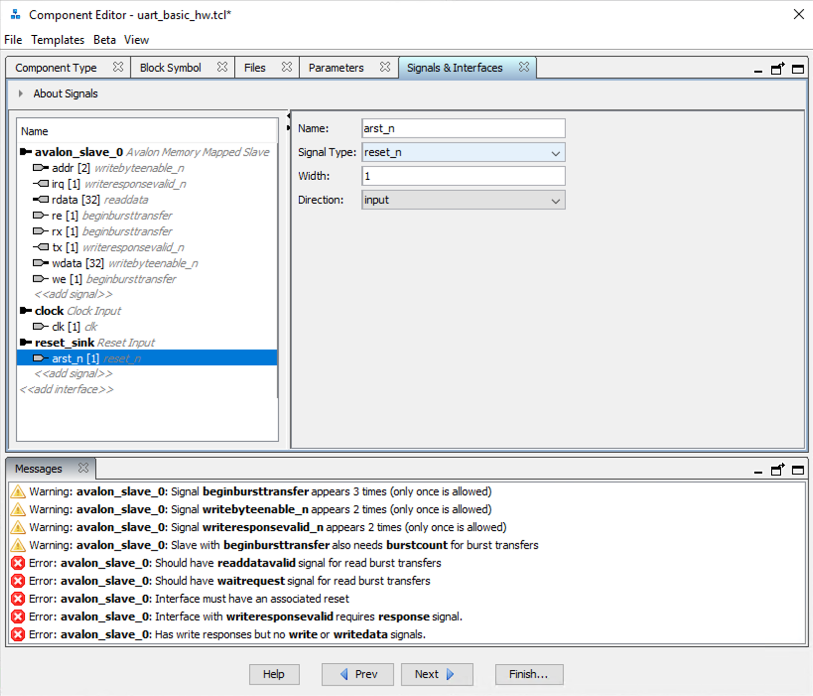
Fig. 60 Change the signal type of the reset signal.#
The TX and RX signals should not be associated with the Avalon slave interface. These signals should be exported out of the CPU system and connected to FPGA pins. The correct interface to use is a Conduit interface. Rename the Conduit interface to uart and add the two signals rx and tx as shown in Fig. 61.
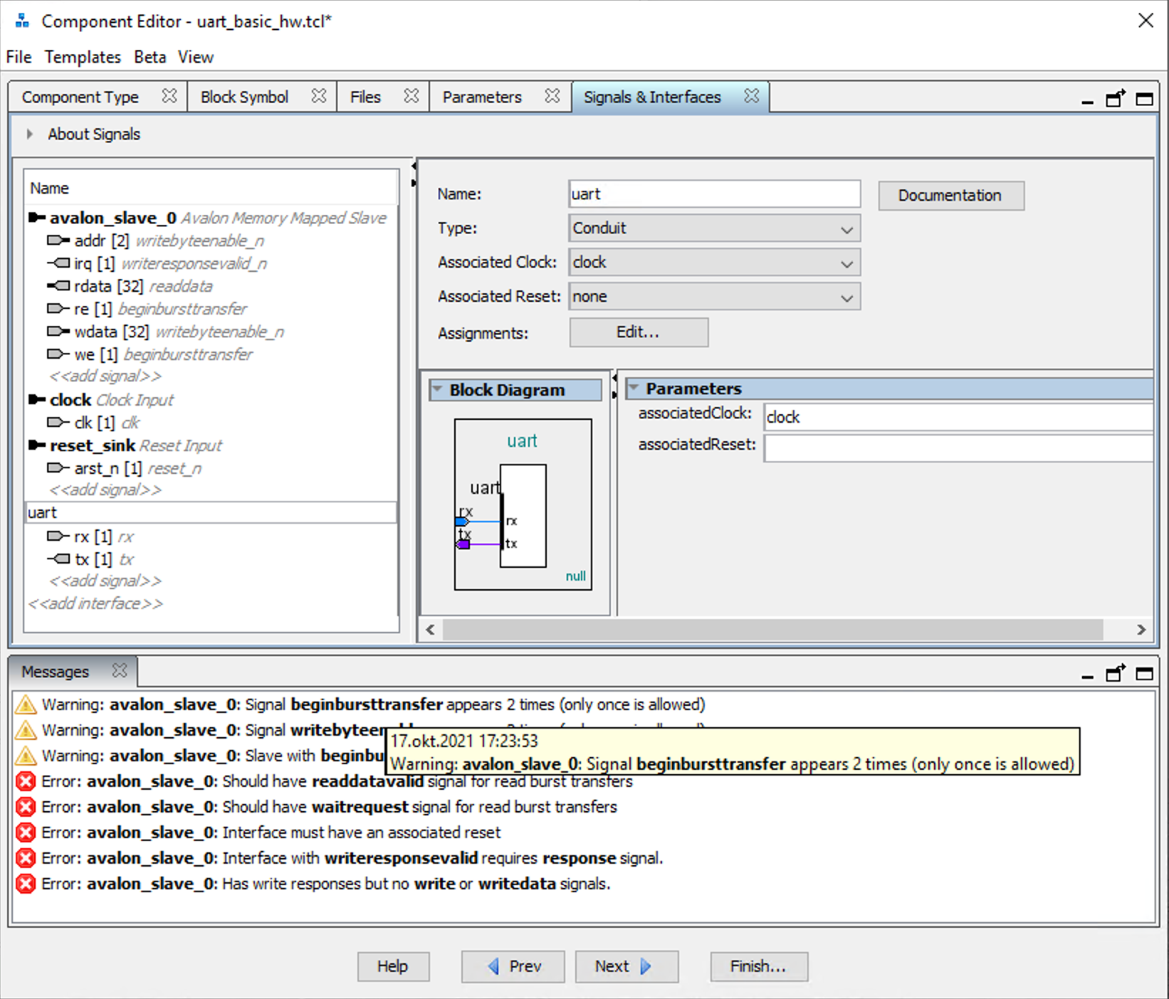
Fig. 61 Add a Conduit interface to export the UART signals out of the CPU system.#
Since these are UART signals that will be exported out of the system, there are no relevant signal types to choose from. Instead you can manually rename the Signal Type to rx and tx respectively, as seen for the rx signal in Fig. 62.
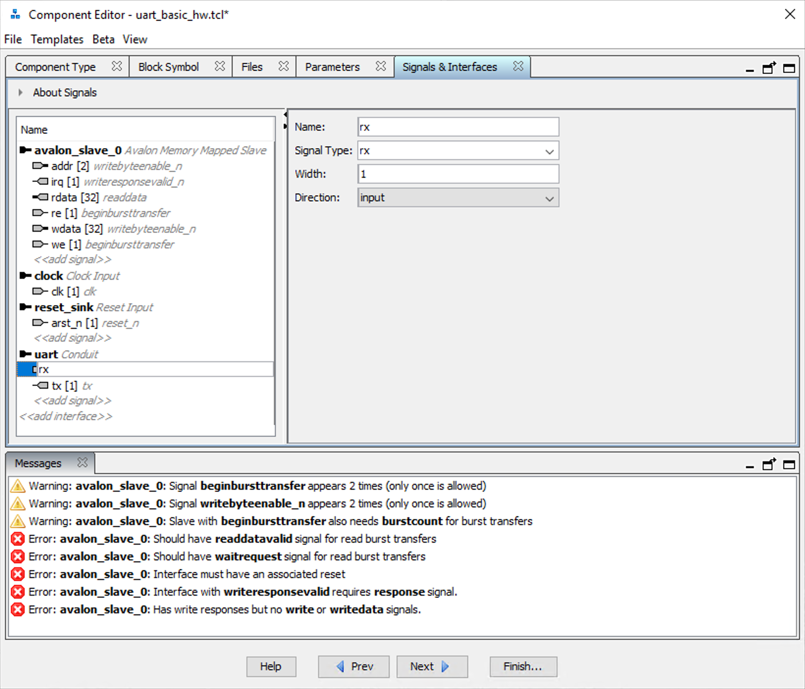
Fig. 62 Change the signal type of the UART signals.#
The last interface to add is the interrupt interface. Since the UART component generates an interrupt that will be sent to the CPU, use an Interrupt Sender interface as shown in Fig. 63. Choose the signal type to be irq.
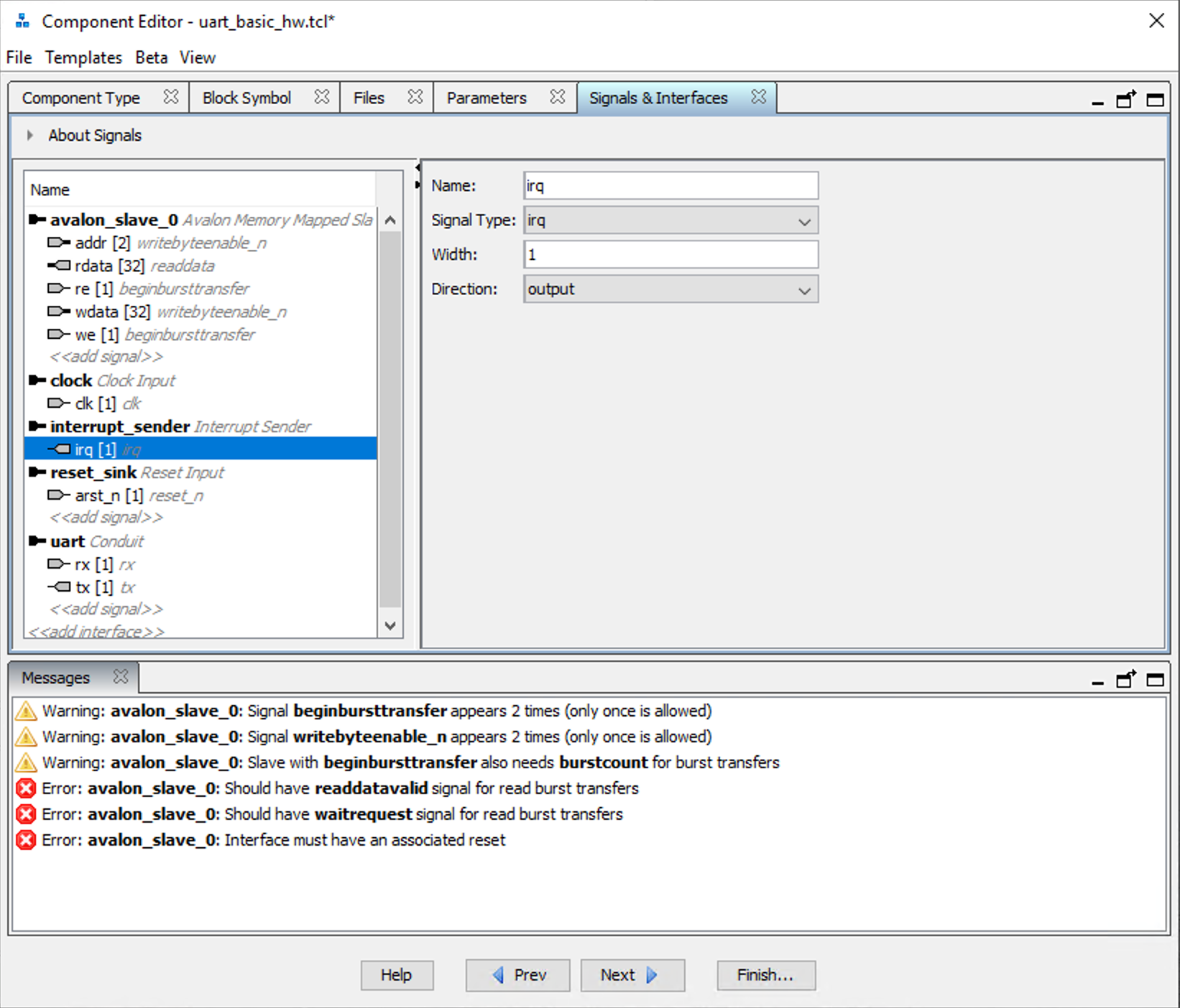
Fig. 63 Add an interrupt sender interface.#
The interrupt must be associated with an addressable Avalon slave interface. Choose avalon_slave_0 as shown in Fig. 64.
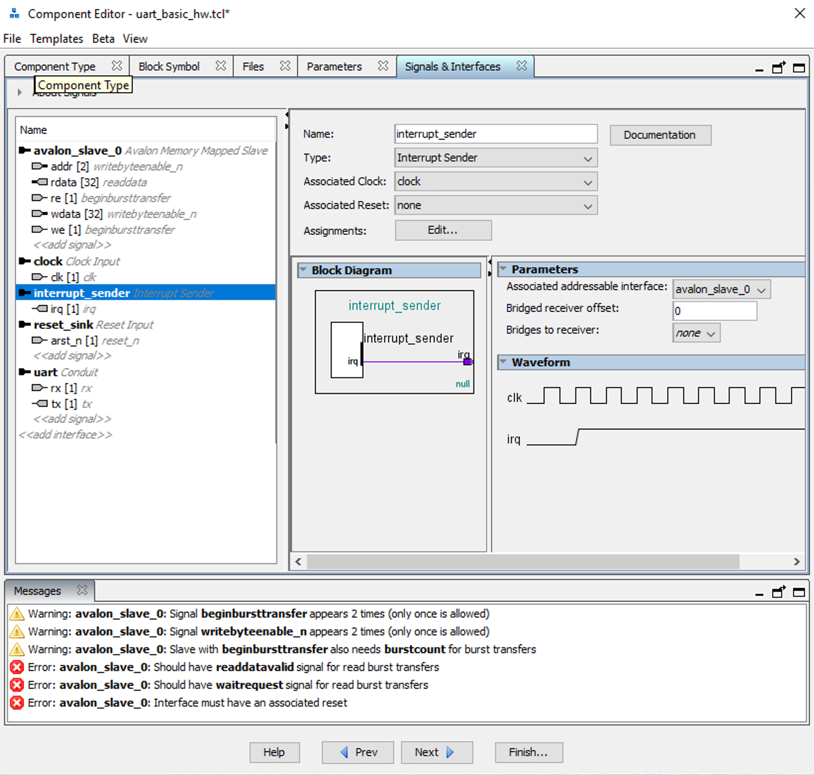
Fig. 64 Associate the interrupt sender to the Avalon interface.#
To complete the signal configuration, set the correct signal types of the signals for the Avalon slave interface as shown in Fig. 65. These are the signals which will be used to read and write data from and to the UART’s register interface. Rename the Avalon slave interface to avalon_slave.
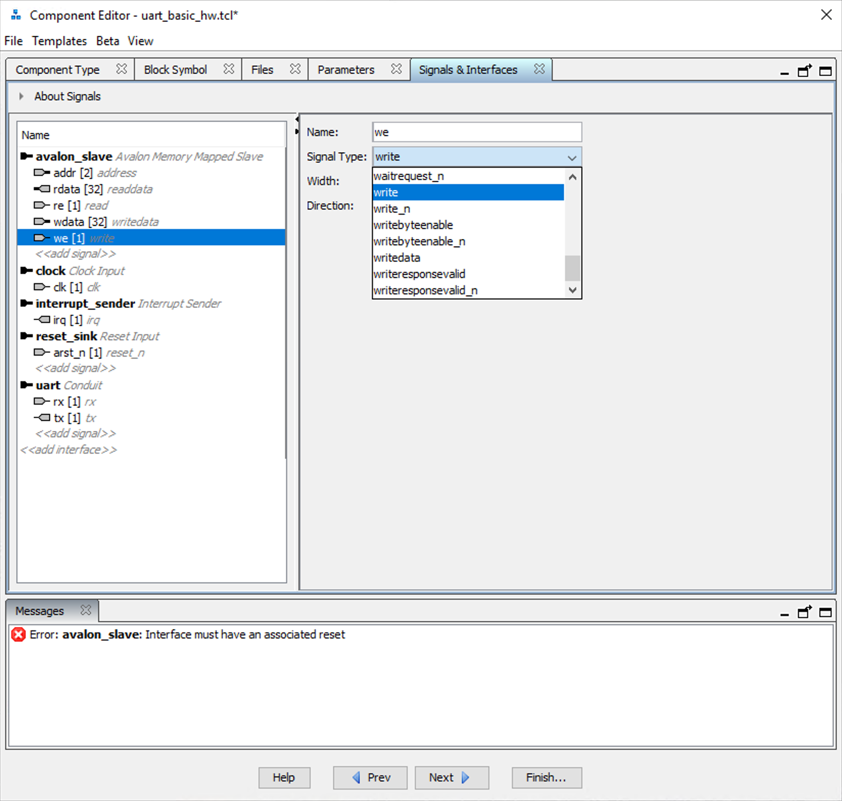
Fig. 65 Set the correct signal types for the signals of the Avalon interface.#
Finally, a reset interface must associted with the Avalon slave interface. Choose the newly added reset interface as shown in Fig. 66.
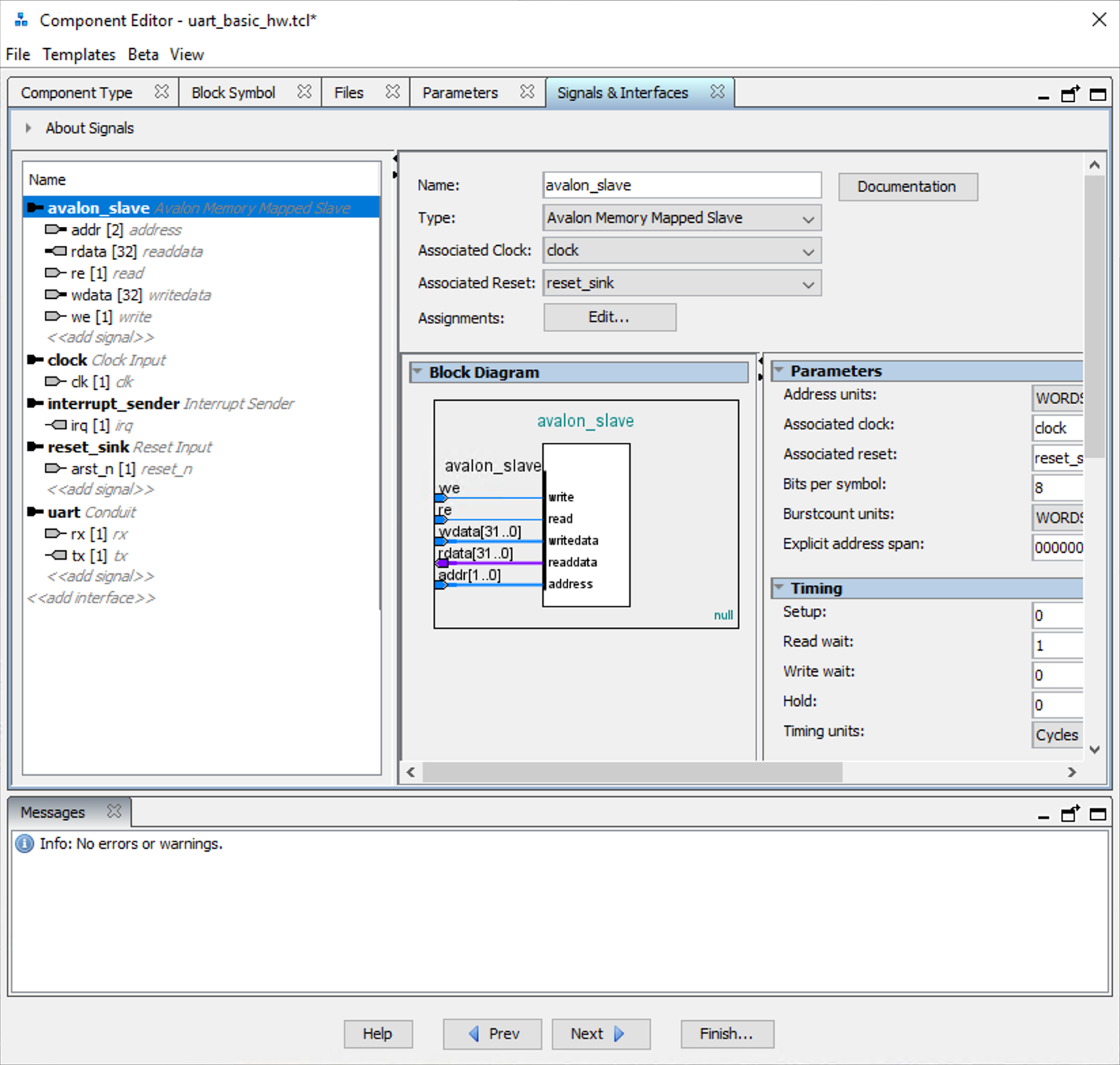
Fig. 66 Associate the reset interface with the Avalon interface.#
After completing the configuration of the UART IP press the Finish button to generate the Hardware Definition file. The file should take the name that was provided in Fig. 54, and will be stored in the Quartus folder project. E.g., uart_basic_hw.tcl.
After refreshing (File–>Refresh system or F5), the UART basic IP should now be available under the FYS4220 group in the IP catalog as shown in Fig. 67.
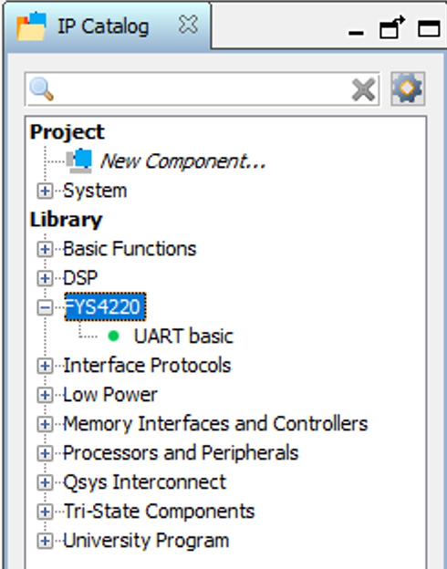
Fig. 67 The newly create UART basic IP is now available in the IP catalog.#
Add the UART module#
In Platform Designer, add and connect the UART module as shown in Fig. 68. Remember to assign an interrupt priority number and to export the UART conduit lines.
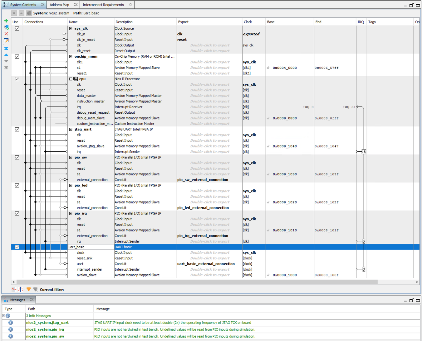
Fig. 68 Add and connect the UART module to the Nios II system.#
Add an SPI module#
The ADXL345 [Deva] digital accelerometer supports serial communication using either SPI (3- and 4-wire) or I2C. For this project we will include an SPI core from the IP catalog as shown in Fig. 69.
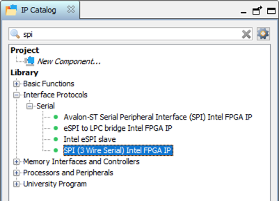
Fig. 69 Choose the SPI (3 Wire Serial) Inter FPGA IP from the IP catalog.#
SPI uses 4 lines to communicate data:
MISO: Master In Slave Out (data from slave to master)
MOSI: Master Out Slave In (data from master to slave)
SCLK: SPI clock
SS_n: Chips select
If more than one slave device is connected to the SPI interface, each slave device requires a separete chip select line. If run in 3-wire mode, only one line is used for data, which means that this data line is bi-directional. In this project we will be using a 4-wire connection with only one slave device. Although the name of the Intel FPGA SPI core specifies 3 Wire Serial, it supports 4-wire communication. E.g., all 4 lines are present in the block diagram in Fig. 70.
Configure the SPI module as shown in Fig. 70. The SPI serial interface will run at a clock frequency of 1 MHz with the required clock polarity and phase settings supported by the ADXL345 accelerometer (see page 15 of the ADXL345 datasheet.[Devb]). For more information about SPI clock polarity and phase settings, read the corresponding section on the SPI wikipedia page. When the clock polarity is 1, the clock idles at 1, e.g., the SPI clock line is high when there is no activity. When the clock phase is set to 1, this means that data is changed on the rising edge of the SPI clock and captured on the falling edge.
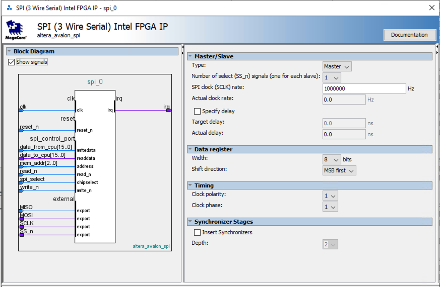
Fig. 70 Configuration window for SPI module. Change the SPI clock frequency to 1 MHz and clock polarity and phase to the value 1.#
Add and connect the SPI module as shown in Fig. 71. Remember to assign the interrupt priority number and to export the UART conduit lines.

Fig. 71 Add and connect the SPI module to the Nios II system.#
Add an Interval Timer#
Most control systems use a timer component to enable precise calculation of time. This timer component generates a periodic timer tick signal that can be used by the CPU to keep track of time. It will set the time resolution for the system’s response time.
Search for and add the Interval Timer module from the IP catalog. Keep the default configuration settings for the component (e.g., timeout of 1 millisecond) as shown in Fig. 72. The interval timer will provide a system clock tick to the CPU every 1 millisecond.
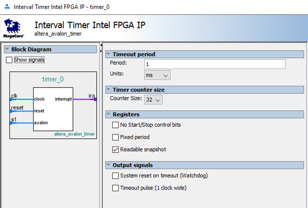
Fig. 72 Configuration window for Interval Timer module.#
Connect the Interval Timer to the system. The purpose of this module is to provide accurate timing, its priority level should therefore be higher than for the other modules. See Fig. 73.

Fig. 73 Add and connect the Interval Timer to the Nios II system.#
Important!
The software drivers for the uC/OS-II real-time kernel expects the Interval Timer module to be named sys_clk_timer. It is therefore highly recommended to use this name. A different name would required manual modifications of the drivers.
Update the PIO interrupt#
The final modification of the system will be to increase the number of inputs to the PIO module that handles interrupts. In Section 3.6 this module was configured with one input and connected to the second push button on the board (KEY1). In addition, we now want to connect the two interrupt lines coming from the ADXL345 accelerometer. Increase the number of inputs to three as show in See Fig. 74.
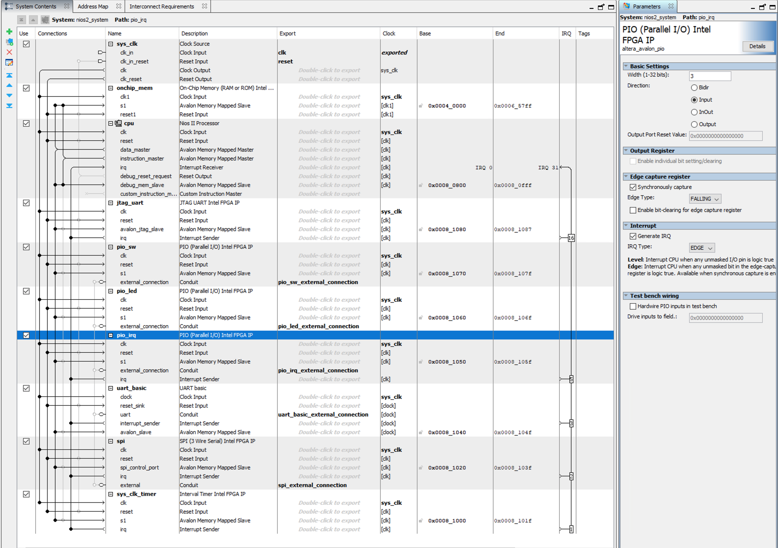
Fig. 74 Increase the number of inputs for the PIO interrupt module to also support the two interrupt lines from the accelerometer.#
Rebuild the hardware#
After making changes to the Nios II system it needs to be regenerated before it can be included in the Quartus project, compiled, and finally downloaded to the FPGA.
Press the “Generate HDL…” to regenerate the system with corresponding VHDL description files.
Top level VHDL#
The newly generated Nios II system has now been extended with additional input and output ports for the UART, SPI, and interrupt interfaces. These new ports must be added to the component declaraction and instantiation of the Nios II system as well as the top level ports of the system_top.vhd. In addition the correct pin assignments must also be made.
Connecting the SPI interface#
The required connections between the MAX 10 FPGA and the accelerometer are shown in Fig. 75. Since the accelerometer supports both SPI and I2C, the lines are labelled accordingly. More information on how to configure the accelerometer for either SPI or I2C communication can be found on page 15 in the ADXL345 datasheet [Devb].
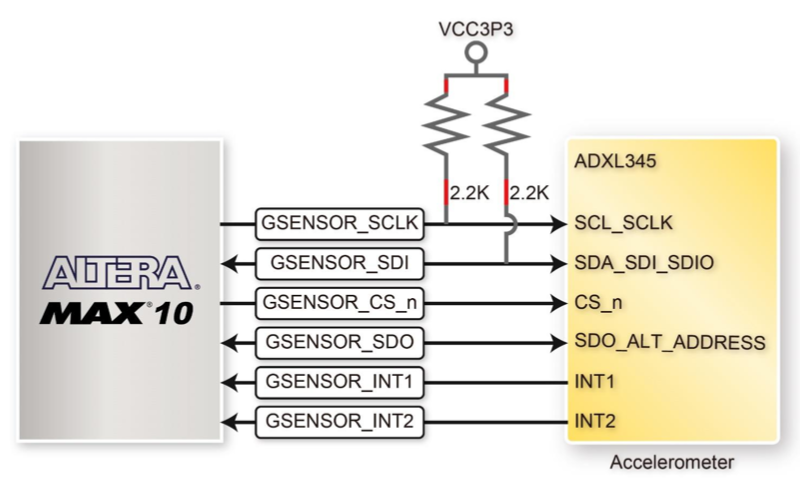
Fig. 75 Connections between the accelerometer sensor and MAX 10 FPGA. Figure 3-24 (p. 39) in the DE10-Lite User Manual`.#
The corresponding FPGA pin numbers can be found on page 40 in the DE10-Lite User Manual [Inc] and is shown in Fig. 76.
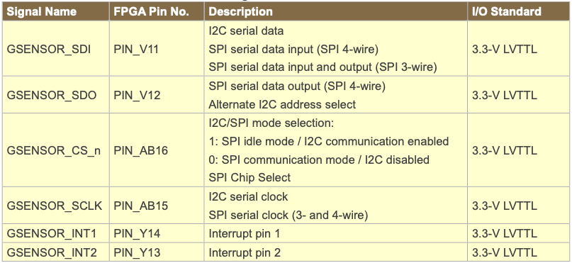
Fig. 76 Pin Assignment for the ADXL345 accelerometer. Table 3-13 (p. 40) in the DE10-Lite User Manuel.#
Add the four SPI ports and the two interrupt ports to the top level VHDL file. Update the pinning Tcl file with the correct pin assignments. The two interrupt pins can be added by expending the already present irq input from Section 3.6 to a standard logic vector of length 3.
Connecting the UART#
The UART will be connected to the host PC using a UART to USB converter cable [Chi] from FTDI Chip. The female pin connectors (TX, RX and GND) can easily be connected to the RaspberryPi header of the DE10-Lite board.
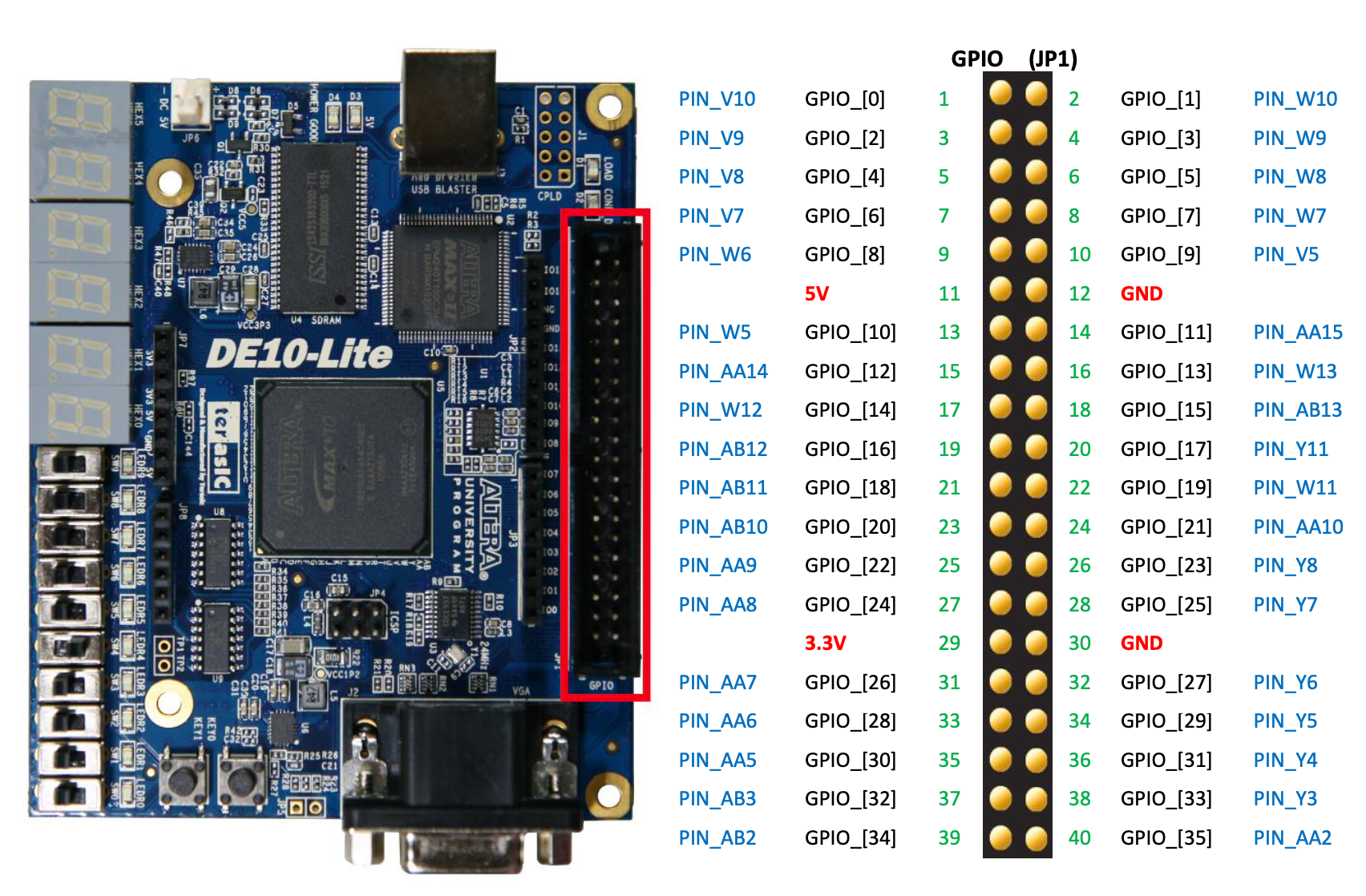
Fig. 77 RaspberryPi header and pin number for the DE10-Lite board. Figure 3-18 in the DE10-Lite User Manual`.#
The ground cable must of course be connected to a ground pin on the pin header, while the RX and TX can be connected to any GPIO pin as long as the correct corresponding pin assignment is performed before compling the Quartus project. The solution example that later will be made available for this project will use:
PIN_V10 as TX
PIN_W10 as RX
Pin 12 as GND.
To identify the orientation of the pin header you can check the back side of the board. Pin number 1 will be marked with a square solder pad as shown in Fig. 78. Checking the pin values with a mulitmeter to identify the ground and voltage supply pins before making any connections can also be useful.
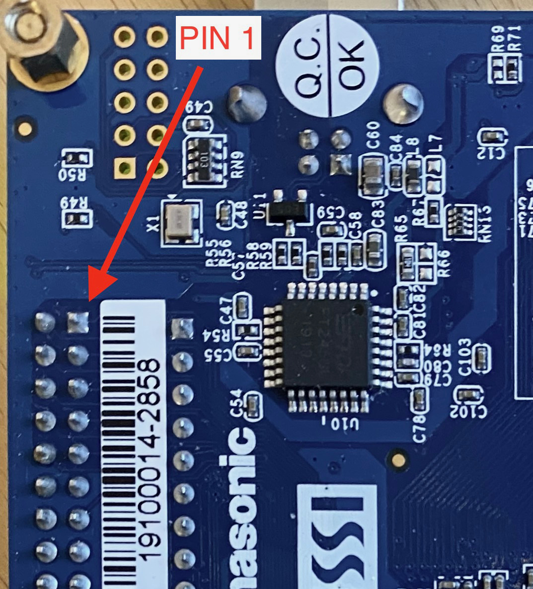
Fig. 78 Backside of the RaspberryPi pin header. Pin 1 is marked using a square solder pad.#
Important
Make sure to carefully read Table 4.2 in the FTDI cable’s datasheet [Chi] to find out which color of the cable corresponds TX, RX or ground.
Remember that the TX on the FPGA side must be connected to the RX on the cable side and vice versa.
AN INCORRECT CONNECTION MAY DAMAGE THE DEVICE! PLEASE DOUBLE CHECK BEFORE MAKING ANY CONNECTIONS.
Add the TX and RX ports to the top level VHDL-file and update the pinning Tcl-file with the correct pin assignments.
Compile the Quartus project#
The updated VDHL design now handles several input signals which are external to the design’s clock domain. A 2-register synchronizer must therefore be added to these signals before you can compile the project.
Which signals need synchronizers?
The RX, SPI_MISO, and all 3 interrupt signals are all external input signals that must be synchronized. An example for the 3 interrupt inputs is shown below.
architecture rtl of system_top is
.
.
.
-- Two synchronization registers for the 3-input interrupts
signal irq_sync_r1 : std_logic_vector(2 downto 0);
signal irq_sync_r2 : std_logic_vector(2 downto 0);
.
.
.
begin

p_sync : process (clk)
  begin
    if rising_edge(clk) then
      -- synchronize interrupt inputs
      irq_sync_r1 <= irq;
      irq_sync_r2 <= irq_sync_r1;
    end if;
  end process;
The irq_sync_r2 must then be connected to the IRQ input in the port map of the microcontroller system.
Make sure to rerun the updated pinning Tcl-script before the Quartus project finally can be compiled to generate a new programming file. Download the new FPGA design to the MAX10 FPGA.
Software#
In this part you will test the recently added UART and SPI interfaces.
To test the UART interface, you will expand the software application to:
Read the rx_data register of the UART module when new data has been received from the host PC. This involves adding the required interrupt handling for UART module.
Send the received data back to the host PC by writing the data to the tx_data register of the UART module.
Use Putty or Screen to send and receive data from the host PC.
To test the SPI interface, you will use the provided SPI drivers to read back the identification number of the ADXL345 accelerometer.
Update the board support package#
Whenever the hardware of the microcontroller system has been changes, it is required to regenerate the board support package. See section Board Support Package for how to do this.
UART loopback test#
The UART loopback test will be performed by sending and receving characters from the host PC over the USB to UART cable. You will implement the required software application to receive and send back these characters.
From the development of the UART controller in P1: UART controller we know that an interrupt will be signaled when data has been received by the UART RX module. You therefore need to add the required interrupt handling to the software application. An example of interrupt handling has already been demonstrated in EX7: Nios II interrupt handling. Use this as a starting point for adding interrupt handling for the UART. Try first to write the required code before looking at the tip provided below.
Tip
The interrupts from the UART are enabled by default. That is, they are automatically set when there is a falling edge on either the tx_busy or rx_busy signal. Thus, there is no need to manually enable interrupts as was done for the example shown in EX7: Nios II interrupt handling. You therefore only need to register the interrupt with the Nios II system using the alt_ic_isr_register function.
alt_ic_isr_register(UART_BASIC_IRQ_INTERRUPT_CONTROLLER_ID,
			UART_BASIC_IRQ, handle_interrupt_uart, uart_status_ptr, 0x0);
The names of the arguments provided here may be different for your design depending on how you named the respective components when designing the system in Platform Designer. These names can be found in the system.h file of the board support package.
To service the interrupt you will need to write a dedicated interrupt handling routine (suggested name handle_interrupt_uart). When called, this routine will:
Read the UART module’s status register and store the value in the volatile int variable uart_status. This is a similar operation as was done for the edge_capture variable from the example in P1: UART controller.
Reset the interrupt bits in the UART module’s status register. This is done by performing a write operation to the UART’s status register.
In the main function, check whether the tx_irq og rx_irq bit has been set.
If the rx_irq bit has been set, read the rx_data register and send back the receive data by writing to the tx_data register.
A shift operation combined with a bitwise AND operation can be used to check if a given bit position is set:
//Check if rx_irq bit is set
if ((uart_status >> 5) & 0x1) {
// read rx_data register and write the returned value to the tx_data register
}
// Reset the status registers IRQ bits.
Using the USB to UART cable#
The UART will be connected to the host PC using a UART to USB converter cable [Chi] from FTDI Chip. The cable has an FT232R chip that converts from TTL UART signals to USB. With the correct FTDI drivers installed, the cable will apear as a virtual COM port (VCP). This then allows us to communicate with the USB interface, and therefore our UART interface on the FPGA, via a standard PC serial emulation port.
When connected, the cable should be visible in the Device Manager or under Devices and Printers in the Windows control panel as shown in Fig. 79 and Fig. 80. If the cable is not visible, you may have to installed the VCP driver.
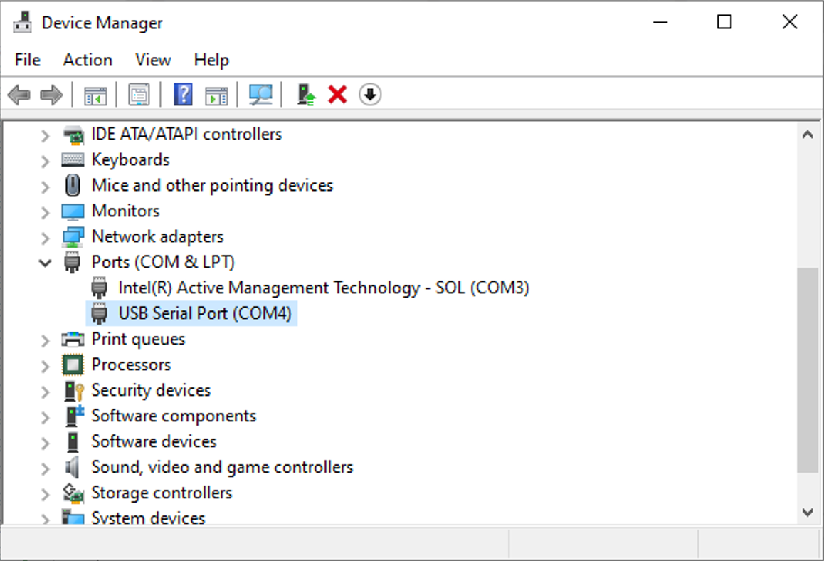
Fig. 79 Windows 10 Device Manager.#
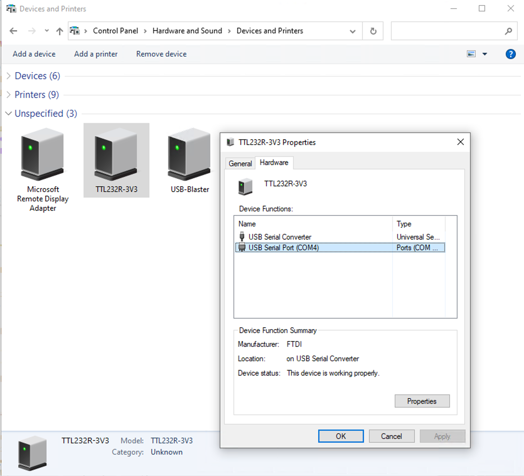
Fig. 80 Windows 10 Devices and Printers. The corresponding COM-port number can be found in the hardware tab under properties when right clicking on the device.#
For Linux and Mac OS, the cable will be listed under the /dev folder as shown in Fig. 81.

Fig. 81 The FTDI cable will show up as TTY device and usually with an extension consisting of usbserial and a serial number.#
The cable can be accessed by opening a serial port using e.g., Putty on windows (Fig. 82) or Screen (Fig. 83) on Linux/Mac OS.
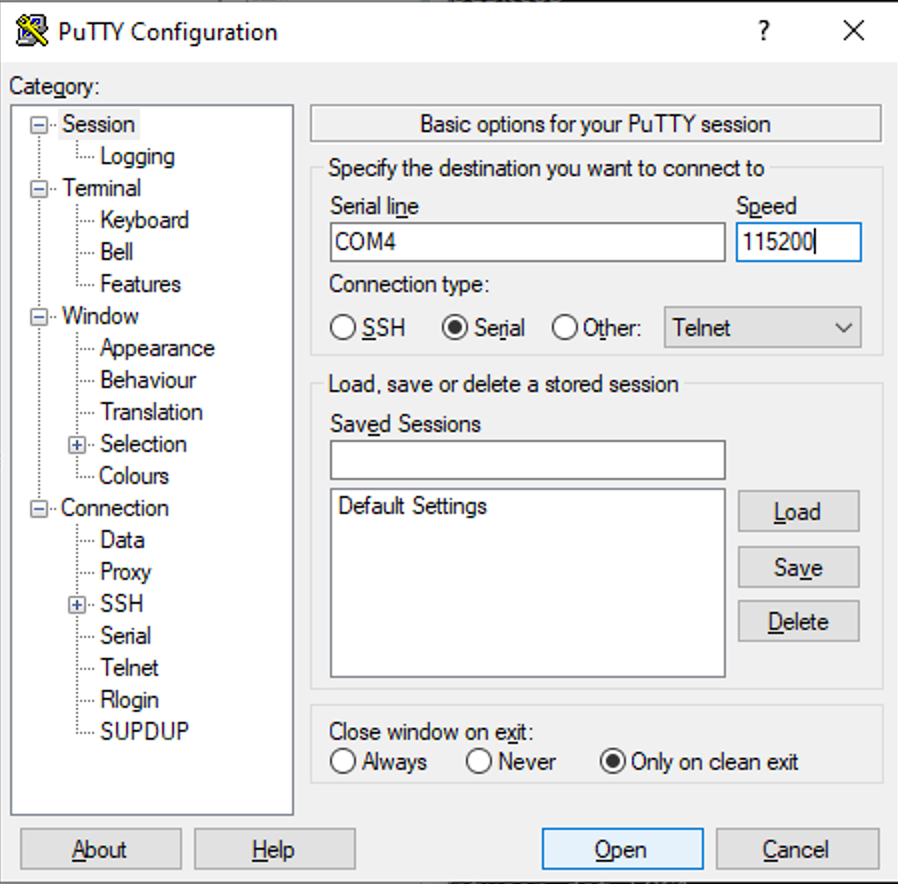
Fig. 82 Putty: choose the correct COM-port and baud rate.#

Fig. 83 Screen can be started from the command line with the device path and baud rates as arguments.#
In Python the cable can be accessed using the PySerial module.
SPI test#
To test the SPI interface you will read back the device identification number from the ADXL345 accelerometer using the SPI IP module added to the microntroller system in Add an SPI module.
SPI driver#
The SPI module comes with a driver that can be used to easily communicate with any attached SPI device. By including the driver’s header file altera_avalon_spi.h, this gives access to function alt_avalon_spi_command shown below.
int alt_avalon_spi_command(alt_u32 base,  // base address of SPI module in Nios II system
                            alt_u32 slave, // slave select line (0 in for this project)
                            alt_u32 write_length, // number of bytes to write
                            const alt_u8* wdata, // pointer to write buffer
                            alt_u32 read_length, // number of bytes to read
                            alt_u8* read_data, // pointer to read buffer
                            alt_u32 flags) // configuration options (0 for this project)
This function is described on page 49 in the Embedded Peripherals IP User Guide [Int21]. It performs a control sequence on the SPI bus. It supports only SPI hosts with a data width less than or equal to 8 bits. A single call to this function writes a data buffer of arbitrary length to the mosi port, and then reads back an arbitrary amount of data from the miso port.
The driver source files can be found in the /app_bsp/drivers/inc and /app_bsp/drivers/src folders.
HAL alternative types
For embedded processors it is often important to know the exact width and precision of data. ANSI C data types are supported when writing software for embedded systems but their widths are dependent on the compiler’s convention. For the Nios II hardware abstraction layer these types are defined in the alt_types.h header file that can be located in the HAL/inc folder of the boad support package project. This header types provides the following alternative type definitions:
typedef signed char  alt_8;
typedef unsigned char  alt_u8;
typedef signed short alt_16;
typedef unsigned short alt_u16;
typedef signed long alt_32;
typedef unsigned long alt_u32;
typedef long long alt_64;
typedef unsigned long long alt_u64;
To declare a 8-bit unsigned variable you can therefore also use:
alt_u8 data;
Defining a variable as int, corresponds to signed 32-bit.
ADXL345 SPI transaction#
Add an SPI module shows how the SPI read transaction wave diagram for the ADXL345. The most significant bit is use to set a write (low) or read condition (high). To read or write multiple bytes in one transaction the MB bit must be set to 1.
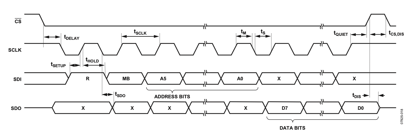
Fig. 84 An SPI read transaction for the ADXL345. Figure 38 on page 39 in the ADXL345 datasheet ADXL345 datasheet. The write transaction can be found on the same page.#
The ADXL345 can be configured support 3-wire and 4-wire SPI by writing respectively 1 or 0 to the corresponding SPI-bit in the DATA_FORMAT register. Our system has been built to support 4-wire SPI with both the MISO and MOSI ports active. Although the datasheet claims that the default reset value of this register is 0x0, which corresponds to 4-wire SPI, some of you may experience that the DEVID register can not be read back correctly without explicitly also first writing to the DATA_FORMAT register.
Write the necessary code to first configure the DATA_FORMAT register to set the SPI bit to support 4-wire SPI, and then read back the DEVID register and print the device ID to the terminal. Register addresses are listed in Table 19 in the ADXL345 datasheet [Devb].
Tip
// tx and rx data buffers
alt_u8 spi_rx_data[6];
alt_u8 spi_tx_data[6];
int no_bytes;

// ADXL345 command byte configuration
// bit 7: RnW (0: Write, 1: Read)
// bit 6: For multi byte read or write from the accelerometer
// bit 5-0: register address

// Configure SPI bit in DATA_FORMAT register
// bit 7: 0 (Write)
// bit 6: Single
spi_tx_data[0] = 0x00 | 0x31; // Single byte write (cmd byte + 1 data byte) + register address
spi_tx_data[1] = 0x0; // register data to write
no_bytes = alt_avalon_spi_command(SPI_BASE,0,2,spi_tx_data,0,spi_rx_data,0);

// To read device ID register send 0x80
spi_tx_data[0] = 0x80 | 0x0; //Single byte read + address
no_bytes = alt_avalon_spi_command(SPI_BASE, 0, 1, spi_tx_data, 1, spi_rx_data, 0);
Remember to include the necessary header files.
#include "alt_types.h"
#include "altera_avalon_spi.h"