EX3: 4-bit up-counter#
The previous exercises demonstrated how to describe purely combinational logic. However, most FPGA designs also make use of synchronous logic. This means that the design also uses the flip-flops (or registers) that can be found in the FPGA’s logic blocks. This allows the output of the combinational operation implemented in the look-up table to be synchronized to a clock signal, as illustrated in figure Fig. 21. The output of the flip-flop is remains constant an active edge of the clock triggers the flip-flop to latch th input value of the register to the register’s output.
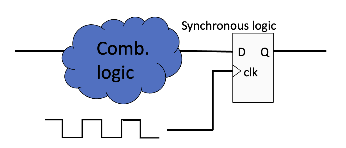
Fig. 21 In synchronous logic the combinational logic is synchronized to a clock signal.#
By adding a feedback loop to the circuit the logic becomes sequential, as illustrated in figure Fig. 22 That is, the output is dependent not only on the present state of the inputs, but also on the previous state. Sequential logic can be used to implement control logic such as finite state machines.
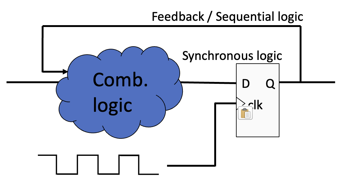
Fig. 22 By adding a feedback loop the ciruit becomes sequential.#
In this exercise you will write the VHDL description for a 4-bit up-counter. A counter is essentially a simple finite state machine where the next value is dependent on the value of the input (‘1’ for an up-counter) and the current value of the counter. Figure Fig. 23 shows a basic block diagram of a counter.
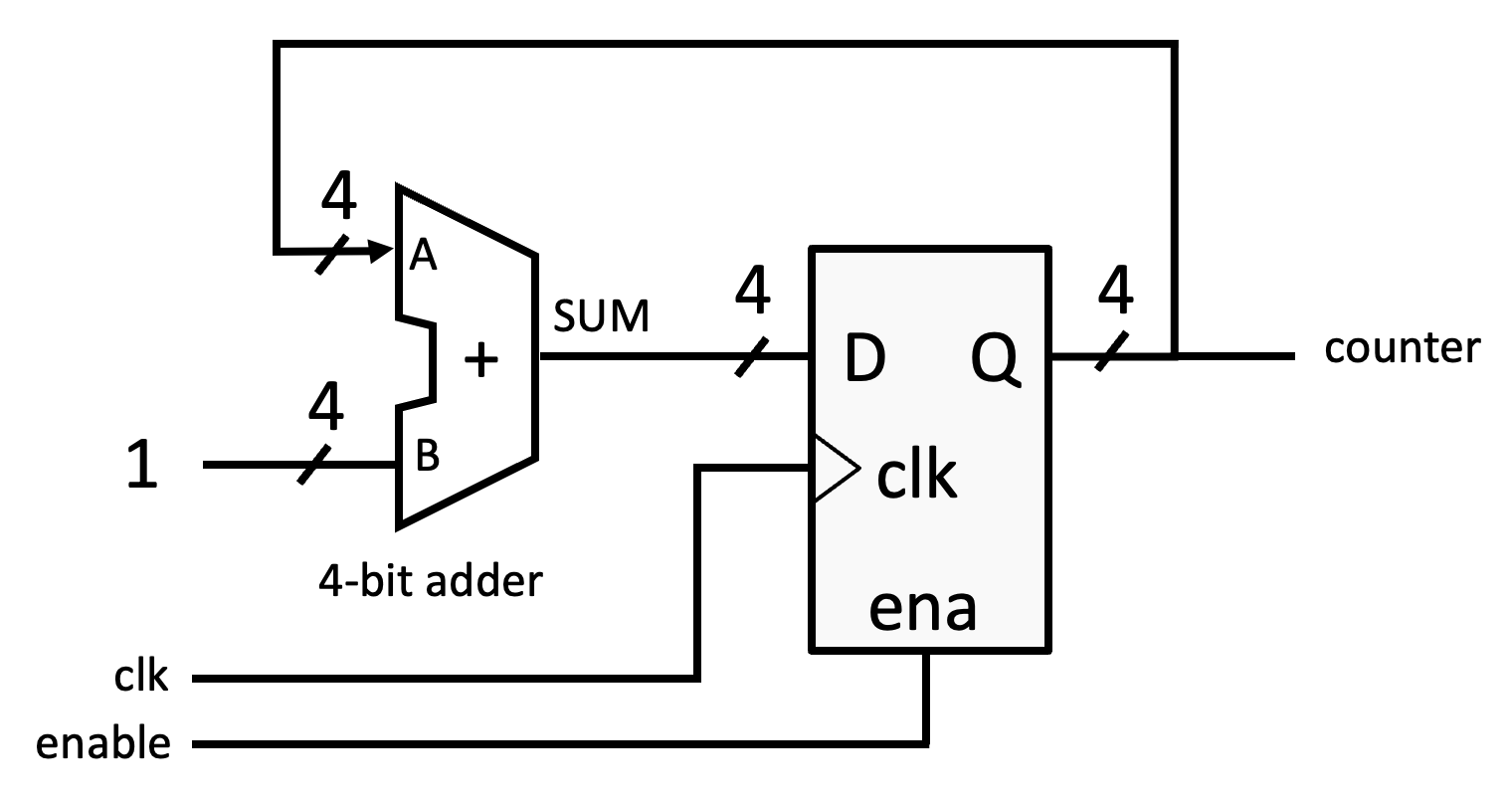
Fig. 23 A basic block diagram of a 4-bit up-counter with an enable signal.#
The learning outcome of this exercise is to:
Be able to implement a basic counter in VHDL using two different approaches: a low level and high level approach. This will help you to better understand the power of the high level VHDL language for designing complex logic circuits.
Be able to use the process statement in VHDL to describe synchronous logic.
Be able to use the unsigned signal type and the IEEE numeric standard library to implement the counter.
Be able to detect the edge of a signal and use it as a counter enable signal
The main functional requirements of the counter are:
The counter shall increment its output by 1 when one of the FPGA board’s push buttons (KEY1) is pressed. That is, the button will act as a count enable.
The count enable signal shall be active high.
The counter design shall run on a clock frequency of 50 MHz (frequency provided by the external clocking circuit on the DE10-Lite board).
The counter shall count from 0 to 15. When the counter reaches 15, the counter shall roll over and the next output value shall be 0.
The counter shall be reset (output shall be 0) when one of the FPGA board´s buttons (KEY0) is pressed. The reset shall be synchronous to the clock signal.
The main test requirements are:
The counter shall be verified using a testbench.
Verify that all valid values of the counter are reached in the correct order.
The duration of the count enable signal shall be longer than 5 system clock cycles.
Verify correct transition from 15 to 0 on the output
Verify that the counter can be reset. This does not have to be done for all values, but verify at least for one other value than 0.
EX3.A: Combinational adder based design#
In the first part of this exercise you will design the counter using the 4-bit adder from the previous exercise.
An up-counter is a piece of logic that increments a value when triggerd by an input condition. When the input condition is not present, the counter needs to store the current value. To store a value in an FPGA a memory element is needed. The most simple memory element that can be used in an FPGA is the flip-flop of the FPGA’s logic block. To implement a register in VHDL, you will need to use a clock triggered process statement. Read more about the process statement in VHDL in the section VHDL Process, and in particular the section on Synchronous process.
Verify the counter in simulation according to the test requirements above. Ask a fellow student to review your testbench and verify your simulation results. This can be done either by asking her/him to inspect your code and results on Github, or by discussing your code and results in person in the lab or on Zoom.
Tip
Both the CIN and COUT ports of the 4-bit full adder are not used in this counter design. CIN is an input and can be driven to ‘0’ directly in the port map. The connection of port COUT also has to be completed in the port map. Since it is not used, it can be specified to be an open connection as shown below.
port map(
        A => counter_i,
        B => "0001",
        CIN => '0',
        COUT => open
        );
Do your design behave as expected?
If your design increments by more than 1 when the enable signal is active, you have probably implemented your design similar to the description below.
p_counter: process(clk)
           begin
             if rising_edge(clk) then
               if enable = '1' then
                  counter <= sum;
               end if;
             end if;
           end process;
Since the process is running on 50 MHz clock, and the enable signal is longer than a clock cycle, the condition enable = '1' will be valid for more than one clock cycle. Thus the flip-flop will update its output more than once for each active pulse on the enable input, resulting in that the counter increments by more than 1.
How can you make sure that the output of the counter will only update once during an enable pulse?
Read the section Metastability and synchronization to find the solution, and particularly the section Edge detection
Design considerations#
The multiplexer shown above is a very simple design and can easily be written using a single process. However, as you design becomes more complex, it is recommended to think about how you can partition you design into multiple processes and even entities/modules. If you include too much logic or functionality within a single process, it may become difficult to read as well as more prone to errors.
Assume that the multiplexer example is to be implemented in hardware, and that the select signal is controlled from an external switch or button.
You will get more experience with this when you start working on the project where you will
EX3.B: High level implementation#
Designing a simple 4-bit up-counter using the combinational 4-bit adder design is not a very effective approach. It is better to make use of the high level features in the VHDL language. In general, an up-counter can be described by the following or similar syntax in most programming languages:
counter = counter + 1
In VHDL we will use a signal object to implement the up-counter. The only syntax difference is to use the language specific assignment operator and add a semicolon at the end.
counter <= counter + 1;
Since this signal is not implemented at the port level of the design, it has to be declared as an internal signal. Arithmetic operations are not supported by the IEEE standard logic 1164 package. The solution is to use the IEEE numeric standard package and declare the signal of type unsigned. Some background on the numeric package here. This package also includes functions to convert between e.g., a standard logic vector and unsigned.
-- include the numeric std library
use ieee.numeric_std.all;

-- Declare the counter signal in the appropriate place
signal counter : unsigned(3 downto 0);
Add the high level description of the counter to your existing code, that is, in parallel to your already existing adder-based design. Connect the output of the high level counter to 4 additional LEDs. In this way you can compare the two counter implementations both in simulation and in hardware.
Compiling the project to hardware#
Before compiling the project you will need to add the new pin assignments to the Tcl-script script file. Remember to re-run the tcl-script before compiling the project. If you have used different identifier names for your port entries, make sure to match them with the one used in the Tcl-file. You will find the correct pin assignment for the push buttons, LEDs, and external 50 MHz clock source in the DE10-Lite user guide.
When compiling the project in Quartus you will notice the following warning ”Timing requirements not met”. This warning indicates that the design now has a register-to-register path that exceeds the clock period. However, we have not yet specified the actual clock period for our design and a default clock period of 1000 MHz have therefore been set by Quartus as a default value.
Verify this setting by opening the compilation report and navigate to the ”Clocks” part of the Timing Analyzer. ”Processing -> Compilation Report” (Ctrl+R) as shown in Fig. 24
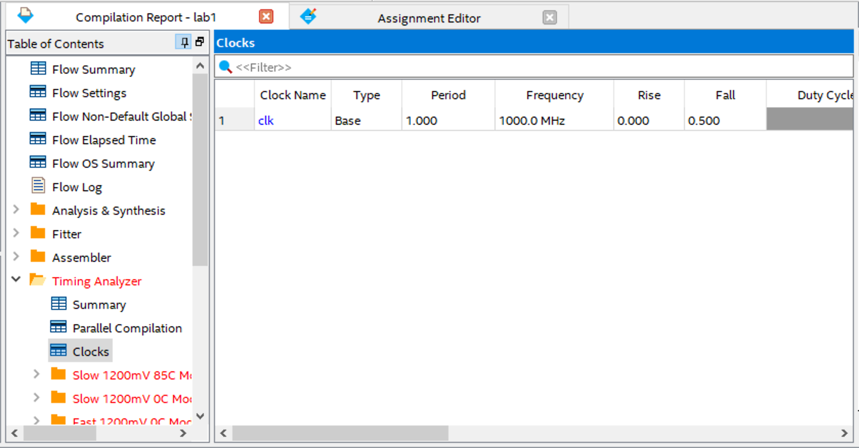
Fig. 24 Compilation report.#
Timing settings are critically important for a successful design. For this tutorial we will specify the correct clock frequency of 50 MHz by creating a basic Synopsys Design Constraints File (.sdc) that the Quartus Prime Timing Analyzer will use during design compilation. A Synopsys Design Constraints File is required by the Timing Analyzer to get proper timing constraints. Without it, the Compiler will not properly optimize the design.
To create an SDC, perform the following steps:
Open the Quartus Prime Timing Analyzer by choosing Tools -> Timing Analyzer.
Create the timing netlist by double clicking on ”Create Timing Netlist” under the Tasks pane.
Choose File -> New SDC file. The SDC editor opens.
Choose ”Edit -> Insert constraint -> Create clock”. This will open the window shown in Fig. 25
Fill in the clock name and correct period value corresponding to 50 MHz.
You willl need to connect this generated clock to an actual target / port in your design. Click the button with the three dots right of the Targets field. Click the List button in the new window that just opened and select the clk port as shown in Fig. 26. The corresponding SDC command is also shown.
Click OK and then Insert and this SDC command will be added to the SDC editor.
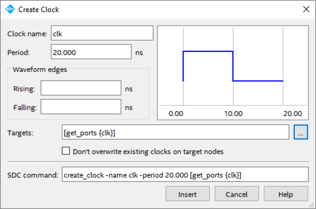
Fig. 25 Create the clock.#
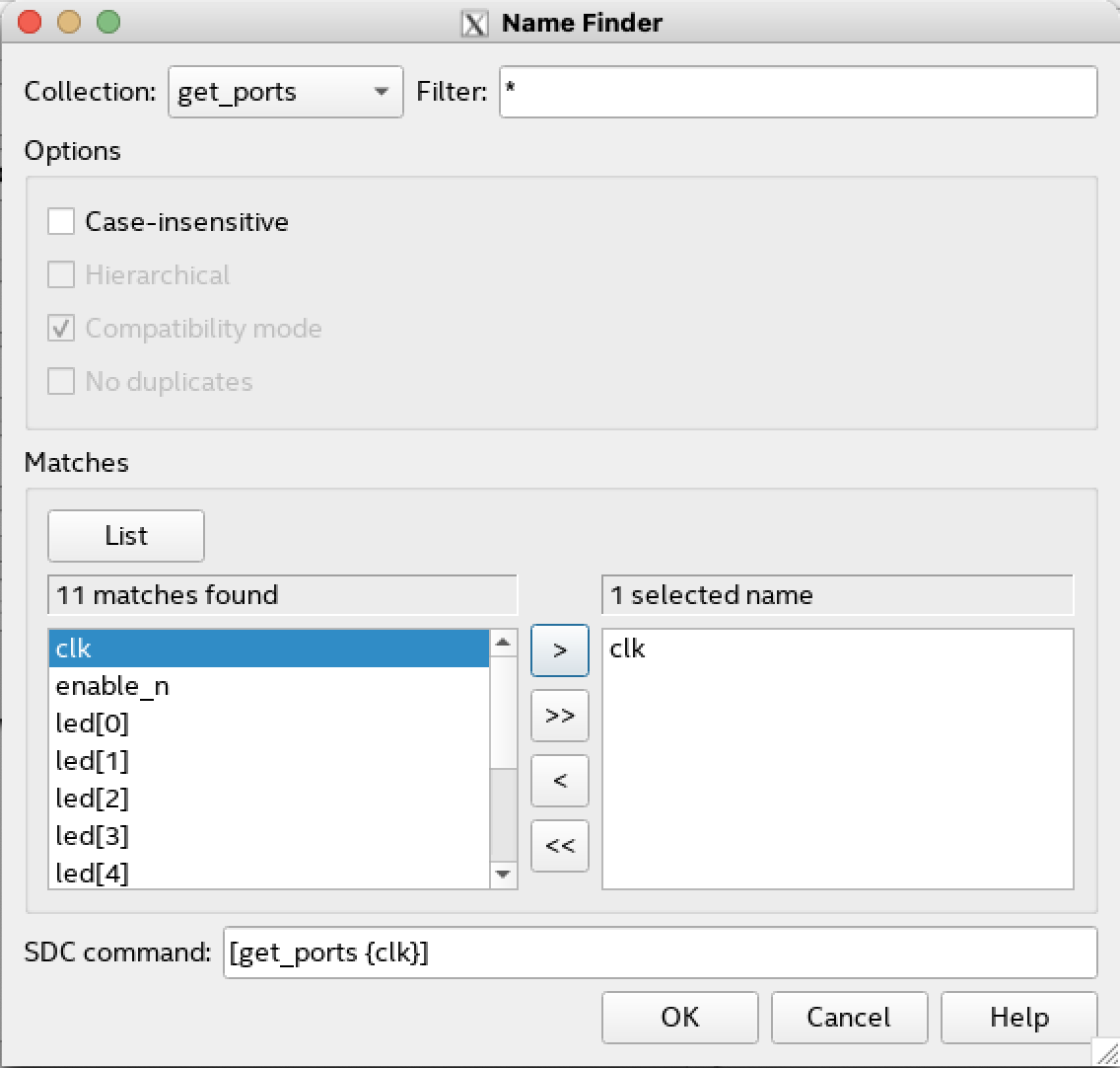
Fig. 26 Select the clock port.#
Save this file in your project directory with the name de10-lite.sdc.
Add this file to the Quartus project: ”Project -> Add current file to project”.
Close the SDC editor window and recompile the Quartus project.
Verify that the warning ”Timing requirements not met” is no longer present and that the clock has been constraint to 50 MHz in the compliation report.
Tip
The short-cut to setting up the clock constraint is to create a file called DE10-lite.sdc in your project directory and then save the the following SDC command in the file.
create_clock -name clk -period 20.000 [get_ports {clk}]
Program the FPGA#
Open the Quartus programmer and download the recompiled design to your FPGA.
Press KEY1 to increment the counters.
Press KEY0 to reset the counters