EX5: A basic Nios II system#
In the following sections we will show a practial example of building a Intel Nios II microcontroller system. While the tools used are specific to the specific hardware and FPGA vendor, the overall concepts should be similar between hardware platforms.
The learning outcome of this problem is to:
Get familiar with the software build tools for Quartus.
Be able to build and generate a basic microcontroller system based on the Nios II soft core processor.
Include this microcontroller design in a top level VHDL description and synthesise the system.
Be able to write, compile, and test a basic “Hello world” program to run on the microcontroller system.
We will start by building the system shown in Fig. 30. The system consist of three main units:
Nios II/e CPU
On-chip memory / RAM
JTAG UART
The CPU and on-chip memory are the two most important components needed to build and run a system, where the on-chip memory is needed to store instructions and data used by the CPU. The JTAG UART is a IP core that provides an easy way to communicate serial character streams between the host PC and the microcontroller system. On the PC host, sending and receiving characters can be done by using the Nios II terminal software (nios2-terminal.exe).
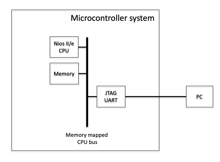
Fig. 30 Simplified overview of a basic Nios II system.#
Warning
The description and scripts provided in this example assumes that you will use the following directory structure:
nios2_example
quartus
hdl
software
The Quartus folder recursively contains all the relevant Quartus project and Platform Designer files. The top-level VHDL file for the project (system_top.vhd) is stored in the hdl folder. Software and board support package files are stored in the software folder.
Example code on Github
The code for this example can be found here: fys4220/fys4220_nios2_example
Building the Hardware#
Start by creating a new Quartus project, give it the name system_top, and choose the correct FPGA device and part number: MAX10 10M50DAF484C7G.
To build the microcontroller system we will use the Platform designer tool from Intel.
In Quartus, go to the menu line and choose Tools –> Platform designer.
Microcontroller system#
When you first open the Platform designer the system will only consist of the Clock source component as show in Fig. 31. This component is responsible for receiving the main clock and reset for the system, and to distribute these to other components in the system.
Double click on this component and make sure that the system clock frequency is set correctly to 50 MHz. By default the Clock source component assumes that reset provided to the system is asynchronous. The type of reset can be set by choosing the appropriate value for Reset synchronous edges. Since we will be using a push button as a reset, leave the choose at None. I.e., an asynchronous reset.
Rename the component to sys_clk. Components can be renamed by right-clicking on the component and choosing rename, or by using the short-cut CTRL-R.
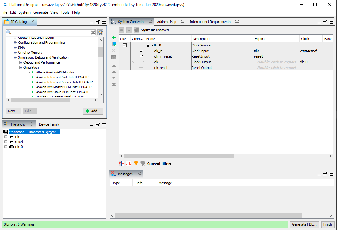
Fig. 31 Platform designer when starting a new build from scratch.#
Additional components can be found and added from the IP Catalog. If you do not see the IP Catalog tab, this can be opened from (View –> IP Catalog). You can either navigate the component tree under Library, or use the search field to find the required component.
On-chip memory#
A microcontroller system will need a memory to store its instructions and data. In the IP catalog, locate the component called On-Chip Memory (RAM or ROM) Intel FPGA IP. Double click the component and it will be added to the system. In its configuration window, set the total memory size to 153600 bytes and uncheck the initialize memory content box. Leave all other settings with their default values. Press Finish and rename the component to onchip_mem.
Important!
It is possible to configure the memory with a pre-built software. This will allow the system to boot and immediatley run without the need to download the software. The corresponding mem.hex file then first needs to be generated by the Nios-II software build tools and referenced here. However, for this problem we will develop the software later and download it separately. We therefore need to uncheck the initialize memory content box.
Nios II Processor core#
Next you will add the Nios-II CPU. When searcing for Nios in the IP Catalog you will see two entries under the Embedded processor branch. Choose the Nios II Processor. The classic is an older legacy version. Double click the component to open the configuration settings and choose the NiosII/e radio button. This is the economy version of the processor for which no license is required. The difference between the two processors are listed in the table below the radio buttons of the configuration tab. Press Finish and rename the component to cpu.
Connecting the components#
After adding the onchip memory and CPU a number of error messages will appear. These can removed by correctly connecting and configuring the newly added components.
The clock source is used to distribute the system clock to the various system components. A connection from the clock source to the on-chip memory and CPU is therefore needed. This is done by connecting the clk output of the clock source component to the clk1 and clk inputs of the on-chip memory and CPU respectively as shown in Fig. 32.
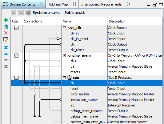
Fig. 32 Connections between components are made by clicking on the open circles in the connections column. Closed or solid circles indicates that a connection has been made.#
The Nios-II CPU uses a Harvard type architecture where the data and instructions are kept in separate memory partitions and can be accessed simultaneously. The CPU therefore has a separate data master and instruction master connections. Since the on-chip memory will store both data and instructions, both have to be connected to the Avalond Memory Mapped Slave input of the on-chip memory component as shown in Fig. 33. Within the on-chip memory the data and instructions are separated and stored at different address partitions.
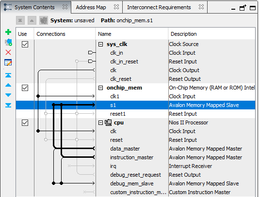
Fig. 33 Connection the data and instruction master connections to the on-chip memory.#
CPU reset and exception vectors#
After the on-chip memory has been connected to the CPU, the reset and exception vector locations have to be correctly configured for the CPU. Double click on the CPU component and navigate to the Vectors tab. Select onchip_mem.s1 for both the reset and exception vector memory. Within the onchip memory the program that you download will by default be located at address position 0x0. This is also the position at which the instruction pointer of the CPU should point to in case of a reset. The corresponding location offset for the excpetion vector is 0x20.
In addition to distributing the clock, the clock source component is also responsible for distributing the reset signals to the system’s other componets. Connect the clk_reset output of the clock source to the reset1 and reset inputs of the onchip memory and cpu respectively.
The remaining error messages refers to that there is an overlap between the location of the data and instruction interfaces. This is a common error that you will see when ever you add a new component to the system that is connected to memory mapped master of the CPU. This can be corrected by either manually changing the base and end address locations of each component or by letting the Platfrom designer automatically assign available address locations to each component (System –> Assign Base address). The latter option is strongly recommend as you do not have to think about which address location to use. At this stage you should have a system with out error messages, and you are ready to add the other needed components.
JTAG UART#
The JTAG UART is a IP core that provides an easy way to communicate serial character streams between the host PC and the microcontroller system. It can also be sused to debug the Nios-II system. It controls the connection between the system and the JTAG-to-USB connection on the board. Use the default settings for this component. Connect the clk, reset as for the other compents. Since the CPU will not fetch instructions from the JTAG UART, only the data master interface of the CPU shall be connected to the memory mappped slave interface of the JTAG UART.
The JTAG UART also has an interrupt interface that shall be connected to the interrupt interface (irq) of the CPU. The IRQ column can be used to set the interrupt priority of the JTAG UART. The lower the number the higher the priority. Since the JTAG UART is related to serial communication and debugging of the system, it will usually not have a high priority during normal operation. Click the corresponding box in the IRQ window and type the value 16.
The Platform designer does provide an Assign Interrupt Numbers command which connects IRQ signals to produce valid hardware results. However, assigning IRQs effectively requires an understanding of how software responds to them. Because the Platform designer does not know the software behavior, the Platform designer cannot make educated guesses about the best IRQ assignment. It is thefore required to set the interrupt prioity levels manually.
Saving the system#
Make sure that all warning and error messages has removed and save the system. Select (File –> Save as) and save as nios2_system.qsys to a relevant directory. E.g., the diretory where you will store your quartus project.
The system should no look similar to Fig. 34.
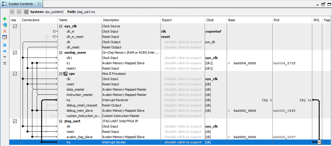
Fig. 34 Connecting the JTAG UART to the system and setting the required prority.#
Generate the HDL#
When all the necessary components are included and connected, it is time to generate the HDL description that will be used by Quartus to synthesize the system.
To generate the HDL description of the system:
Press the Generate HDL button or choose Generate–>Generate HDL from the menu line.
Choose VHDL under “Create HDL design files for synthesis”.
Disable “Create block symbol file (.bsf)”.
Leave “Create simulation model” as None.
Press Generate.
A directory with the same name as the system (in our case nios2_system) will now contain an HDL description of the system.
The Platform Designer creates four files of particular interest and importance:
nios2_system.qsys
The Platform Designer file. This file must be kept under version control.
nios2_system/nios2_system_inst.vhd
An instantiation template generated when the system is saved
nios2_system/synthesis/nios2_system.qip
This file includes all the information needed to synthesize the the system in your Quartus project. This file must be included in the Quartus project.
nios2_system.sopc
This file includes all the information needed for the Nios II software build tools to generate the required Board Support Package (BSP).
Tip
If you make changes the system in the Platform Designer, you must remember to regenerate the system (e.g., HDL, qip and SOPC files).
Since the system can be fully generated from the .qys files, this is the only file that needs to be kept under version control.
Top-level HDL#
After the microcontroller system has been generated it is time to include it in your top-level VHDL description.
The nios2_system_inst.vhd contains a template for the system instantiation as shown below:
 component nios2_system is
    port (
        clk_clk       : in std_logic := 'X'; -- clk
        reset_reset_n : in std_logic := 'X'  -- reset_n

end component nios2_system;

 u0 : component nios2_system
    port map (
        clk_clk       => CONNECTED_TO_clk_clk,       --   clk.clk
        reset_reset_n => CONNECTED_TO_reset_reset_n  -- reset.reset_n
    )
The same information can also be shown if choosing (Generate –> Show Instantiation Template), and can be used to instantiate the microcontroller system in your top-level HDL as show below.
library ieee;
use ieee.std_logic_1164.all;

entity system_top is
  port (
    clk : in std_logic;
    arst_n : in std_logic
  );
end entity;

architecture rtl of system_top is

  component nios2_system is
    port (
      clk_clk : in std_logic := 'X'; -- clk
      reset_reset_n : in std_logic := 'X' -- reset_n
    );
  end component nios2_system;

begin

  u0 : component nios2_system
    port map(
      clk_clk => clk, --   clk.clk
      reset_reset_n => arst_n -- reset.reset_n
    );
  end architecture;
Copy and past the top-level description of system_top into a file called system_top.vhd. Store the file in the hdl folde and add it to your project. (Project–>Add/Remove Files in Project).
Adding remaining necessary files#
The Platform Designer creates a file called nios2_system.qip when it generates the HDL description for the system. This file includes all the information needed to synthesize the the system in your Quartus project. It therefore needs to be added to your Quartus project. In Quartus choose (Project–>Add/Remove Files in Project), navigate to the folder containing the .qip file and add it.
The last step needed is to add the relevant pinning and timing constraints:
# system_top.sdc

create_clock -name clk -period 20.000 [get_ports {clk}]
derive_clock_uncertainty
# de10-lite_pinning.tcl

# Dedicated FPGA clock pin for 50 MHz clock
set_location_assignment PIN_P11 -to clk

# key0 - used as reset
set_location_assignment PIN_B8 -to arst_n

#To avoid that the FPGA is driving an unintended value on pins that are not in use:
set_global_assignment -name RESERVE_ALL_UNUSED_PINS_WEAK_PULLUP "AS INPUT TRI-STATED"
Place the system_top.sdc and de10-lite_pinning.tcl file in the quartus folder.
Add both files to your Quartus project and run the pinning Tcl-script (Tools–>Tcl Scripts). Verify that the correct pinning assignments have been made in the Assignments Editor (Assignments–>Assignments Editor).
Save and compile the Quartus project.
Building the Software#
In this part you will write a basic “Hello, World!” application. A microcontroller system’s software applications usually consists of an application project and a Board Support Package (BSP) project. The BSP is a layer of software containing hardware-specific drivers and routines that that can be used by the main software application to acccess the specific hardware resources of the system. This usually comprises a set of C or C++ source and header files.
In this example it provides easy access to the JTAG UART for writing characters between the system and host PC, simply by using a printf statement.
The software application you will implement is shown below:
// File: app.c

#include <stdio.h>

int main(){
    printf("Hello, World!\n");
    return 0;
}
Intel provides a graphical user interface for developing a Nios II software application – Nios II Sofware Build Tools for Eclipse. This can be started from Quartus (Tool–>Nios II Sofware Build Tools for Eclipse). However, this Eclipse-based GUI is very slow and sometimes buggy, which makes it a cumbersome experience to work with. A much better approach is to use the available command line tools:
nios2-bsp (generates BSP)
nios2-app-generate-makefile (generates software application makefile)
Board Support Package#
Open the Nios II command shell from the main Windows menu (In Linux it can be started by writing nios2_command_shell.sh in a terminal window).
Navigate to the software-folder of your project and create the folder app_bsp:
cd software
mkdir app_bsp
Create the board support package using the following command:
nios2-bsp hal app_bsp ../quartus/nios2_system.sopcinfo
For more information on how to use the nios2-bsp command type nios2-bsp --help:
$ nios2-bsp --help

Usage: nios2-bsp <bsp-type> <bsp-dir> [<sopc>] [--<option>]*
To create a BSP you will need to specify the type of Hardware Abstraction Layer (see Section 3.4) to use, the path to were the BSP will be stored, and the path to the SOPC information file generated by the Platform Designer. The SOPC information file will be used to generate the relevant hardware-specific drivers for the system we generated in Building the Hardware.
Available BSP-types are hal and ucosii. hal is the basic abstraction layer when running a bare metal Nios II application. That is, an application without an operating system. The ucosii BSP-type supports a software application that is running on the real-time kernel $\mu&C/OS-II.
To compile the BSP, navigate to the app_bsp folder and type make:
$ make
Software application#
Create the folder software/app and add the file app.c with the c-code already provide above in Building the Software.
From the software folder create the software application makefile by typing:
nios2-app-generate-makefile.exe --bsp-dir app_bsp --src-dir app --app-dir app
Again, to learn more about how to use the nios2-app-generate-makefile.exe, type nios2-app-generate-makefile.exe --help.
$ nios2-app-generate-makefile.exe --help
Command: nios2-app-generate-makefile

Usage: nios2-app-generate-makefile --bsp-dir <directory> [<options>]
Compile the software application by navigating to the app folder and type make:
$ make
Info: Building ../app_bsp
C:/intelFPGA_lite/18.1/nios2eds/bin/gnu/H-x86_64-mingw32/bin/make --no-print-directory -C ../app_bsp
[BSP build complete]
Info: Compiling app.c to obj/default/./app.o
nios2-elf-gcc -xc -MP -MMD -c -I../app_bsp/HAL/inc -I../app_bsp -I../app_bsp/drivers/inc  -pipe -D__hal__ -DALT_NO_INSTRUCTION_EMULATION -DALT_SINGLE_THREADED    -O0 -g -Wall   -mno-hw-div -mno-hw-mul -mno-hw-mulx -mgpopt=global  -o obj/default/./app.o app.c
Info: Linking app.elf
nios2-elf-g++  -T'../app_bsp/linker.x' -msys-crt0='../app_bsp/obj/HAL/src/crt0.o' -msys-lib=hal_bsp -L../app_bsp   -Wl,-Map=app.map   -O0 -g -Wall   -mno-hw-div -mno-hw-mul -mno-hw-mulx -mgpopt=global  -o app.elf obj/default/./app.o -lm -msys-lib=m
nios2-elf-insert app.elf --thread_model hal --cpu_name cpu --qsys true --simulation_enabled false --stderr_dev jtag_uart --stdin_dev jtag_uart --stdout_dev jtag_uart --sopc_system_name nios2_system --sopcinfo c:/Users/ketilroe/workspace/nios2-example/software/app_bsp/../../quartus/nios2_system.sopcinfo
Info: (app.elf) 28 KBytes program size (code + initialized data).
Info:           114 KBytes free for stack + heap.
Info: Creating app.objdump
nios2-elf-objdump --disassemble --syms --all-header app.elf >app.objdump
[app build complete]
This will create the executable file app.elf [1], which will be downloaded to run on the microcontroller system.
Programming the FPGA#
Hardware#
To download and test the sofware application you first need to configure the FPGA with the hardware system from Building the Hardware. This can be done either through the Programmer application in Quartus (Tools–>Programmer), or from the Nios II command shell.
nios2-configure-sof <relative_path_to/configuration_file.sof>
Example
E.g., if in software/app folder and .sof file is quartus/output_files:
$ nios2-configure-sof ../../quartus/output_files/system_top.sof
Info:   *******************************************************************
Info: Running Quartus Prime Programmer
Info: Command: quartus_pgm --no_banner --mode=jtag -o p;C:/Users/   ketilroe/workspace/nios2-example/quartus/output_files/system_top.sof
Info (213045): Using programming cable "USB-Blaster [USB-0]"
Info (213011): Using programming file C:/Users/ketilroe/workspace/  nios2-example/quartus/output_files/system_top.sof with checksum   0x00401269 for device 10M50DAF484@1
Info (209060): Started Programmer operation at Sun Oct 10 17:18:34 2021
Info (209016): Configuring device index 1
Info (209017): Device 1 contains JTAG ID code 0x031050DD
Info (209007): Configuration succeeded -- 1 device(s) configured
Info (209011): Successfully performed operation(s)
Info (209061): Ended Programmer operation at Sun Oct 10 17:18:36 2021
Info: Quartus Prime Programmer was successful. 0 errors, 0 warnings
Info: Peak virtual memory: 4425 megabytes
Info: Processing ended: Sun Oct 10 17:18:36 2021
Info: Elapsed time: 00:00:03
Info: Total CPU time (on all processors): 00:00:0
Download application software#
When the FPGA has been configured, you can download the software using the following command:
nios2-download -g <relative_path_to/application.elf>
Example
E.g., if in sofware folder
$ nios2-download -g app/app.elf
Using cable "USB-Blaster [USB-0]", device 1, instance 0x00
Pausing target processor: OK
Initializing CPU cache (if present)
OK
Downloaded 29KB in 0.3s (96.6KB/s)
Verified OK
Starting processor at address 0x00040230
Test application sofware#
The main task of the software application is to write “Hello, World!” to the standard output. In the board support package, the standard output is configured to be the JTAG UART. To access the JTAG UART on the host PC we use the nios2-terminal command line application:
$ nios2-terminal.exe
nios2-terminal: connected to hardware target using JTAG UART on cable
nios2-terminal: "USB-Blaster [USB-0]", device 1, instance 0
nios2-terminal: (Use the IDE stop button or Ctrl-C to terminate)

Hello, World!