EX2: Adder#
The goal of this exercise is to design and simulate a 4-bit full adder. The adder will add two 4-bit values defined by the slide switches and show the result on the LEDs.
The learning outcome of this exercise is to:
Be able to describe basic combinational logic with VHDL.
Be able to simulate your design using a basic VHDL test bench and Modelsim
Be able to partition your design in sub-units and combine then using a structural design.
Before you start to write code it is always recommended to first spend some time to think about and plan how you want to solve the problem. It can e.g., be helpful to draw a basic block diagram or schematic to outline your design.
The exercise is divided into 3 parts:
EX2.A: 1-bit half adder
EX2.B: 1-bit full adder
EX2.C: 4-bit full adder
Create and check out a new branch called ex2 for this exercise. Make sure to commit and push your work regularly, e.g., after each sub-assignment. A pull request should be created after all the sub-assignments have been completed.
EX2.A: 1-bit half adder#
In the previous exercise you were introduced to the Quartus Prime Lite design tool, and you learnt how to build your first FPGA project and program the FPGA. The design was very simple, connecting an input directly to an output. In this exercise you will now see how you can use VHDL to write combinational logic. We will use the example of a half-adder. Create a new Quartus Prime Lite project and write the necessary VHDL code to implement a half adder. Test the adder in hardware. Remember to update the pinning information.
EX2.B: 1-bit full adder with simulation#
Expand your half adder design to also include a carry in signal, adding the necessary statements to make it into a full adder.
In the previous exercises you have tested and verified your design directly in hardware. This is not the recommended method of working. It is instead good practice to always verify your design through simulations before testing in hardware. This is achieved using testbenches written in VHDL. Make sure to study the section Testbenches before you continue. Use the knowledge gained from that section to build a testbench for your full adder design.
EX2.C 4-bit full adder with simulation#
Use the 1-bit full adder from the previous exercise to design a 4-bit adder. Make use of the structural design approach to reuse the full adder as a component. It will be helpful to draw a block diagram to better see how the various inputs and outputs will be connected. Create a testbench to verify the 4 bit adder.
The 4-bit adder shall have two 4-bit inputs, one 4-bit output for the sum, and one 1-bit carry out. The carry in (CIN) will not be used and shall be tied to ground.
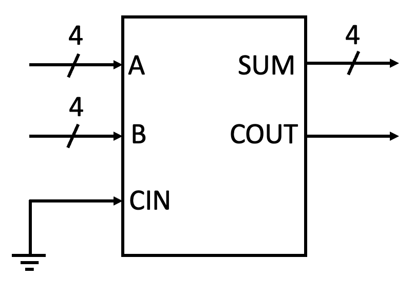
Fig. 20 A 4-bit adder with carry out. Carry in is tied to ground.#
When you have a correctly working 4-bit adder, prepare a new Quartus project and test the adder in hardware. Remember to update the pinning information.
If you want, you can try to implement the adder as specified in the bonus exercises below.
Bonus exercise
For the 4-bit adder above, you have to reuse the 1-bit adder 4 times. This is reasonable feasible. But what if you wanted to implement a 32-bit counter. It would still be possible to individually instantiate 32 1-bit adders, but with all the additional code lines there is also a higher risk of introducting an error. Since this is a rather repetitive task, it is a good candidate for using a loop to generate the 32 instances. Read the section on Generic map and see if you can manage to implement the 4-bit adder using a for generate statement. That is, create an n-bit adder, where n is used to specify the number of bits.
Create a pull request to complete the exercise.#
Create a pull request and remember to add the course instructor as assignee and reviewer if you want the code reviewed.